Download
1 / 61
610 likes | 719 Views
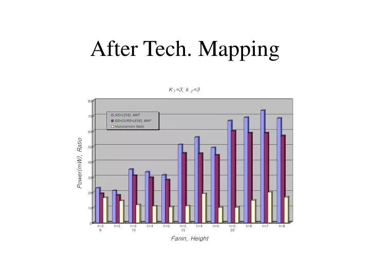
After Tech. Mapping. 7. Circuit Level Design. Delay analysis of buffer chain. Delay analysis considering parasitic capacitance,C p. Buffer Chain. Ck,Pk: stage k buffer output 의 total capacitance, power PT: buffer chain 의 power consumption Pn: load capacitance CL 의 power consumption

E N D
Delay analysis of buffer chain Delay analysis considering parasitic capacitance,Cp Buffer Chain Ck,Pk: stage k buffer output의 total capacitance, power PT: buffer chain의 power consumption Pn: load capacitance CL의 power consumption Eff: power efficiency pn/pT
Determining rise/fall time Slew Rate
Slew Rate(Cont’d) • Power consumption of Short circuit current in Oscillation Circuit
Reducing Area/Power Macro cell(Large part in chip area) XOR/XNOR/MUX(Primitive) Pass Tr. Logic Not using charge/discharge scheme Appropriate in Low Power Logic Pass Tr logic Family CPL (Complementary Pass Transistor Logic) DPL (Dual Pass Transistor Logic) SRPL (Swing Restored Pass Transistor Logic) CPL Basic Scheme Inverter Buffering Pass Transistor Logic
DPL Pass Tr Network + Dual p-MOS Enables rail-to-rail swing Characteristics Increasing input capacitance(delay) Increasing driving ability for existing 2 ON-path equals CPL in input loading capacitance SRPL Pass Tr network + Cross coupled inverter Restoring logic level Inverter size must not be too big Pass Transistor Logic(Cont’d)
Using Precharge/Evaluation scheme Family Domino logic NORA(NO RAce) logic Characteristics Decreasing input loading capacitance Power consumption in precharge clock Increasing useless switching in precharging period Basic architecture of Domino logic Dynamic Logic
Reorder the equivalent inputs to a transistor based on critical path delays and power consumption N- input Primitive CMOS logic symmetrical in function level antisymmetrical in Tr level capacitance of output stage body effect Scheme The signal that has many transition must be far from output If it is hard to estimate switching frequency, we must determine pin ordering considering path and path delay balance from primary input to input of Tr. Example of N-input CMOS logic Input Pin Ordering Experimentd with gate array of TI For a 4-input NAND gate in TI’s BiCMOS gate array library (with a load of 13 inverters), the delay varies by 20% while power dissipation by 10% between a good and bad ordering
VDD A B C D MPD MPA MPB MPC CL 1 1 A MNA CB 1 1 1 1 B MNB CC 1 1 1 1 C MNC CD 1 1 D MND (a) (b) (c) (d) INPUT PIN Reordering Simulation result ( tcycle=50ns, tf/tr=1ns) : A가 critical input인 경우 =38.4uW, D가 critical input인 경우 =47.2uW
Example Definition sensitization : input signal that forces output transition event sensitization vector : the other inputs if one signal is sensitized Sensitization
Considering Sensitization in Combinational logic:Remove unnecessary transitions in the C.L Considering Sensitization in Sequential logic: Also reduces the power consumption in the flip-flops. Sensitization(Cont’d)
TTL level signal CMOS input Characteristic Curve of CMOS Inverter TTL-Compatible
CMOS output signal TTL input Because of sink current IOL, CMOS gets a large amount of heat Increased chip operating temperature Power consumption of whole system TTL Compatible(Cont’d)
INPUT PIN Reordering • To reduce the power dissipation one should place the input with low transition density near the ground end.(a) If MNA turns off , only CL needs to be charged(b) If MND turns off , all CL, CB, CC and CD needs to be charged (c) If the critical input is rising and placed near output node, the initial charge of CB, CC and CD are zero and the delay time of CL discharging is less than (d) (d) If the critical input is rising and placed near ground end, the charge of CB, CC and CD must dischagge before the charge of CL discharge to zero
저전력 Booth Multiplier 설계 성균관대학교 전기전자컴퓨터공학부 김 진 혁, 이 준 성, 조 준 동
Modified Booth 곱셈기 • Multibit Recoding을 사용하여 부분합의 갯수를 1/2로 줄여 고속의 곱셈을 가능하게 한다. • 피승수(multiplicand) : X , 승수(multiplier) : Y • Recoded digit = Y2i-1 + Y2i -2Y2i+1 ( Y-1=0 ) < Generation and operation of recoded digit >
Modified Booth 곱셈기 - 예 • Example
Multipliers - Area • 16-bit Multiplier Area
Multiplier - Delay • Average Power Dissipation (16-bit)
Multiplier - Power • Worst-Case Delay (16-bit)
Instruction Level Power Analysis • Estimate power dissipation of instruction sequences and power dissipation of a program • Eb : base cost of individual instructions Es : circuit state change effects • EM : the overall energy cost of a program Bi : the base cost of typeiinstruction Ni : the number of typei instruction Oi,j : the cost occurred when a type i instruction is followed by a type jinstruction Ni,j : the number of occurrences when a type i instruction is immediately followed by a typej instruction
Instruction ordering • Develop a technique of operand swapping • Recoding weight : necessary operation cost of operands • Wtotal : total recoding weight of input operand Wi : weight of individual recoded digit i in Booth Multiplier Wb : base weight of an instruction Winter : inter-operation weight of instructions • Therefore, if an operand has lower Wtotal , put it in the second input(multiplier).
Conclusion % of instances with circuit states effects 9.0% reduction Power[pJ] 12.0% reduction 4.0% reduction bits bits
Device Scaling of Factor of S • Constant scaled wire increases coupling capacitance by S and wire resistance by S • Supply Voltage by 1/S, Theshold Voltage by 1/S, Current Drive by 1/S • Gate Capaitance by 1/S, Gate Delay by 1/S • Global Interconnection Delay, RC load+para by S • Interconnect Delay: 50-70% of Clock Cycle • Area: 1/S2 • Power dissipation by 1/S - 1/S2 • ( P = nCVdd2f, where nC is the sum of capacitance times #transitions) • SIA (Semiconductor Industry Association): On 2007, physical limitation: 0.1 m 20 billion transistors, 10 sqare centimeters, 12 or 16 inch wafer
Delay Variations at Low-Voltage • At high supply voltage, the delay increases with temperature (mobility is decreasing with temperature) while at very low supply voltages the delay decreases with temperature (VT is decreasing with temperature). • At low supply voltages, the delay ratio between large and minimum transistor widths W increases in several factors. • Delay balancing of clock trees based on wire snaking in order to avoid clock-skew. In this case, at low supply voltages, slightly VT variations can significantly modify the delay balancing.
Quarter Micron Challenge • Computers/peripherals (SOC): 1996 ($50 Billion) 1999 ($70 Billion) • Wiring dominates delay: wire R comparable to gate driver R; wire/wire coupling C > C to ground • Push beyond 0.07 micron • Quest for area(past), speed-speed (now), power-power-power(future) • Accelerated increases of clock frequencies • Signal integrity-based tools • Design styles (chip + packages) • System-level design(system partitioning) • Synthesis with multiple constraints (power,area,timing) • Partitioning/MCM • Increasing speed limits complicate clock and power distribution • Design bounded by wires, vias, via resistance, coupling • Reverse scaling: adding area/spacing as needed: widening, thickening of wires, metal shielding & noise avoidance - adding metal
CLOCK POWER CONSUMPTION • Clock power consumption is as large as the logic power; Clock Signal carrying the heaviest load and switching at high frequency, clock distribution is a major source of power dissipation. • In a microprocessor, 18% of the total power is consumed by clocking • Clock distribution is designed as a hierarchical clock tree, according to the decomposition principle.
Dynamic Effects on Skew Capacitance Coupling Supply Voltage Deviation (Clock driver and receiver voltage difference) Capacitance deviation by circuit operation Global and local temperature Layout Issues: clocks routed first Must aware of all sources of delay Increased spacing Wider wires Insert buffers Specialized clock need net matching Two approaches: Single Driver, H-tree driver Gated Clocks: The local clocks that are conditionally enabled so that the registers are only clocked during the write cycles. The clock is partitioned in different blocks and each block is clocked with its own clock. Gating the clocks to infrequently used blocks does not provide and acceptable level of power savings Divide the basic clock frequency to provide the lowest clock frequency needed to different parts of the circuit Clock Distribution: large clock buffer waste power. Use smaller clock buffers with a well-balanced clock tree. Solution for Clock Skew
DRIVER for PADS or LARGE CAPACITANCES Off-chip power (drivers and pads) are increasing and is very difficult to reduce such a power, as the pads or drivers sizes cannot be decreased with the new technologies.
Dynamic Power Dissipation Low Power Process
Crosstalk • In deep-submicron layouts, some of the netlengths for connection between modules can be so long that they have a resistance which is comparable to the resistance of the driver. • Each net in the mixed analog/digital circuits is identified depending upon its crosstalk sensitivity • 1. Noisy = high impedance signal that can disturb other signals, e.g., clock signals. • 2. High-Sensitivity = high impedance analog nets; the most noise sensitive nets such as the input nets to operational amplifiers. • 3. Mid-Sensitivity = low/medium impedance analog nets. • 4. Low-Sensitivity = digital nets that directly affect the analog part in some cells such as control signals. • 5. Non-Sensitivity = The most noise insensitive nets such as pure digital nets, • The crosstalk between two interconnection wires also depends on the frequencies (i.e., signal activities) of the signals traveling on the wires. Recently, deep-submicron designs require crosstalk-free channel routing.
Power Measure in Layout • The average dynamic power consumed by a CMOS gate is given below, where C_l is the load capacity at the output of the node, V_dd is the supply voltage, T_cycle is the global clock period, N is the number of transitions of the gate output per clock cycle, C_g is the load capacity due to input capacitance of fanout gates, and C_w is the load capacity due to the interconnection tree formed between the driver and its fanout gates. • Pav = (0.5 Vdd2) / (Tcycle Cl N) = (0.5 Vdd2) / (Tcycle (Cg + Cw )N) • Logic synthesis for low power attempts to minimize SUMi Cgi Ni • Physical design for low power tries to minimize SUMi Cwi Ni • . Here Cwi consists of Cxi + CsI, where Cxi is the capacitance of net i due to its crosstalk, and CsI is the substrate capacitance of net i. For low power layout applications, power dissipation due to crosstalk is minimized by ensuring that wires carrying high activity signals are placed sufficiently far from the other wires. Similarly, power dissipation due to substrate capacitance is proportional to the wirelength and its signal activity.
이중 전압을 이용한 저전력 레이아웃 설계 성균관대학교 전기전자컴퓨터공학부 김 진 혁, 이 준 성, 조 준 동
목 차 • 연구목적 • 연구배경 • Clustered Voltage Scaling 구조 • Row by Row Power Supply 구조 • Mix-And-Match Power Supply 구조 • Level Converter 구조 • Mix-And-Match Power Supply 설계흐름 • 실험결과 • 결론
연 구 목 적 및 배경 조합회로의 전력 소모량을 줄이는 이중 전압 레이아웃 기법 제안 이중 전압 셀을 사용할 때, 한 cell row에 같은 전압의 cell이 배치되면서 증가하는 wiring 과 track 의 수를 줄임 최소 트랜지스터 개수를 사용하는 Level Converter 회로의 구현 • 디바이스의 성능을 유지하면서 이중 전압을 사용하는 Clustered Voltage Scaling [Usami, ’95]을 적용 • 제안된 Mix-And-Match Power Supply 레이 아웃 구조는 기존의 Row by Row Power Supply [Usami, ’97] 레이 아웃 구조를 개선하여 전력과 면적을 줄임
Clustered Voltage Scaling • 저전력 netlist 를 생성
구 조 비 교 Conventional RRPS MAMPS Circuit
Level Converter 구조 • Transistor의 갯수 : 6개 4개 • 전력과 면적면에서 효과적 기 존 제 안