Download

1 / 23
230 likes | 443 Views
MEMS 5-in-1 RM Slide Set #5. Reference Materials 8096 and 8097 The MEMS 5-in-1 Test Chips – Strain Gradient Measurements. Physical Measurement Laboratory Semiconductor and Dimensional Metrology Division Nanoscale Metrology Group MEMS Measurement Science and Standards Project.

E N D
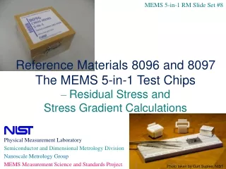
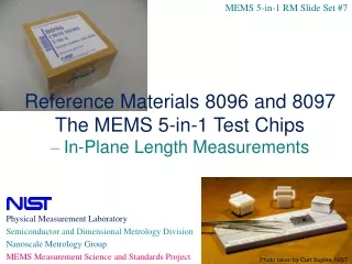
MEMS 5-in-1 RM Slide Set #5 Reference Materials 8096 and 8097 The MEMS 5-in-1 Test Chips – Strain Gradient Measurements Physical Measurement Laboratory Semiconductor and Dimensional Metrology Division Nanoscale Metrology Group MEMS Measurement Science and Standards Project Photo taken by Curt Suplee, NIST
Outline for Strain Gradient Measurements
1. References to Consult • Overview 1. J. Cassard, J. Geist, and J. Kramar, “Reference Materials 8096 and 8097 – The Microelectromechanical Systems 5-in-1 Reference Materials: Homogeneous and Stable,” More-Than-Moore Issue of ECS Transactions, Vol. 61, May 2014. 2. J. Cassard, J. Geist, C. McGray, R. A. Allen, M. Afridi, B. Nablo, M. Gaitan, and D. G. Seiler, “The MEMS 5-in-1 Test Chips (Reference Materials 8096 and 8097),” Frontiers of Characterization and Metrology for Nanoelectronics: 2013, NIST, Gaithersburg, MD, March 25-28, 2013, pp. 179-182. 3. J. Cassard, J. Geist, M. Gaitan, and D. G. Seiler, “The MEMS 5-in-1 Reference Materials (RM 8096 and 8097),” Proceedings of the 2012 International Conference on Microelectronic Test Structures, ICMTS 2012, San Diego, CA, pp. 211-216, March 21, 2012. • User’s guide (Section 4, pp. 76-95) 4. J.M. Cassard, J. Geist, T.V. Vorburger, D.T. Read, M. Gaitan, and D.G. Seiler, “Standard Reference Materials: User’s Guide for RM 8096 and 8097: The MEMS 5-in-1, 2013 Edition,” NIST SP 260-177, February 2013 (http://dx.doi.org/10.6028/NIST.SP.260-177). • Standard 5. ASTM E 2246-11e1, “Standard Test Method for Strain Gradient Measurements of Thin, Reflecting Films Using an Optical Interferometer,” September 2013. (Visit http://www.astm.org for ordering information.) • Fabrication 6. The RM 8096 chips were fabricated through MOSIS on the 1.5 µm On Semiconductor (formerly AMIS) CMOS process. The URL for the MOSIS website is http://www.mosis.com. The bulk-micromachining was performed at NIST. 7. The RM 8097 chips were fabricated at MEMSCAP using MUMPs-Plus! (PolyMUMPs with a backside etch). The URL for the MEMSCAP website is http://www.memscap.com. • Miscellaneous 8. J. C. Marshall, “MEMS Length and Strain Measurements Using an Optical Interferometer,” NISTIR 6779, National Institute of Standards and Technology, August 2001.
2a. Strain Gradient Overview • Definition: The through-thickness variation of the residual strain in the structural layer before it is released • Purpose: To determine the maximum distance that a MEMS component can be suspended, say, in air, before it begins to bend or curl • Test structure: Cantilever • Instrument: Interferometric microscope or comparable instrument • Method: Three data points (from one data trace) are obtained along the length of the cantilever that bends out-of-plane. The strain gradient for this data trace is calculated using these data points and taking into account misalignment. The strain gradient is the average of the strain gradient values obtained from multiple data traces.
2b. Strain Gradient Equation (for one trace) where sgstrain gradient sgtstrain gradient from trace “t” Rintradius of the circle used to characterize the shape of the topmost surface of the cantilever sgcorrectionlength-dependent strain gradient correction term
2c. Data Sheet Uncertainty Equations • Strain gradient combined standard uncertainty, ucsg, equation where uWdue to variations across the width of the cantilever uzresdue to the resolution in the z-direction of the interferometer uxcaldue to the calibration uncertainty in the x-direction uxresdue to the resolution in the x-direction of the interferometer uRavedue to the sample’s surface roughness unoisedue to interferometric noise ucertdue to the uncertainty of the value of the step height standard used for calibration urepeat(shs) due to the repeatability of measurements taken on the step height standard
2c. Data Sheet Uncertainty Equations • Continued…. where udriftdue to the amount of drift during the data session ulineardue to the deviation from linearity of the data scan ucorrectiondue to the uncertainty of the correction term urepeat(samp)due to the repeatability of similar strain gradient measurements • The data sheet (DS) expanded uncertainty equation is where k=2 is used to approximate a 95 % level of confidence.
2c. Data Sheet Uncertainty Equations where For RM 8097, the value for sg is reported (not an “effective” value) and sgcorrection is used for a given length. • Effective value for RM 8096 due to: • Multiple SiO2 layers • Excessive curvature
2d. ROI Uncertainty Equation UROI expanded uncertainty recorded on the Report of Investigation (ROI) UDS expanded uncertainty as obtained from the data sheet (DS) Ustability stability expanded uncertainty
3. Location of Cantilever on RM Chip (The 2 Types of Chips) • RM 8097 • Fabricated using a polysilicon multi-user surface-micromachining MEMS process with a backside etch • Material properties of the first or second polysilicon layer are reported • Chip dimensions: 1 cm x 1 cm • RM 8096 • Fabricated on a multi-user 1.5 µm CMOS process followed by a bulk-micromachining etch • Material properties of the composite oxide layer are reported • Chip dimensions: 4600 µm x 4700 µm Lot 95 Lot 98
3a. Location of Cantilever on RM 8096 Top view of a cantilever Locate the cantilever in this group given the information on the NIST-supplied data sheet 12 12
3b. Location of Cantilever on RM 8097 Lot 95 Lot 98 Top view of two cantilevers Locate the cantilever in this group given the information on the NIST-supplied data sheet
L metal2 (m2) dimensional marker a b exposed silicon to be etched (design layers include active area, contact, via, and glass) c d e Edge 1 Edge 2 Edge 3 y x 4a. Cantilever Description (For RM 8096) etch stop (n-implant encompassing active area) Top view of a cantilever
4b. Cantilever Description (For RM 8097) These “tabs” are not present in the strain gradient group on Lot 98. (The original intent was to keep the same anchor design as used in the Young’s modulus group, but these tabs make it more difficult to locate traces a and e.) Top view of a cantilever (Lot 95)
5. Calibration Procedure • Calibrate instrument in the z-direction • As specified for step-height calibrations • Calibrate instrument in the x- and y-directions • As specified for in-plane length calibrations
6. Measurement Procedure t indicates the data trace (e.g., a or e) • Five 2D data traces are extracted from a 3D data set • For Traces a and e • Enter into the data sheet • The uncalibrated value (x1uppert) for Edge 1 • To find xupper • The x value that most appropriately locates the upper corner of the transitional edge is called xupper or x1uppera for Edge 1 with Trace a • The value for n1t • The maximum uncertainty associated with the identification of xupper is ntxrescalx • If it is easy to identify one point, nt = 1 • For a less obvious point that locates the upper corner, nt > 1 • The uncalibrated values for ya and ye • Determine the uncalibrated endpoint Note: With 0 orientation, all x-values should be > x1ave xres = uncalibrated resolution in x-direction
Edge 1 (x1uppera, ya) Δx Trace a Δy α (x1uppere, ye) Trace e 6. Measurement Procedure (continued) • Determine the misalignment angle, • For Traces b, c, and d • Eliminate the data values at both ends of the trace (all data outside and including Edges 1 and 2) • Choose 3 representative data points (sufficiently separated) • Enter the 3 points into the data sheet (x1, z1), (x2, z2), (x3, z3) • For a 0 orientation, x1ave < x1 < x2 < x3 • For a 180 orientation, negate the x values of all the points such that x1ave > x1 > x2 > x3 > x2ave
Edge 1 x2 calx x3 calx x1 calx f=x1ave calx Trace a α g h i v 6. Measurement Procedure (continued) • Account for the misalignment angle, , and the x-calibration factor • The v-axis is assumed to be aligned with respect to the in-plane length of the cantilever • x1ave, x1, x2, and x3 become f, g, h, and i, respectively, along the v-axis f=x1avecalx g=(x1calxf)cos+f h=(x2calxf)cos+f i=(x3calxf)cos+f
6. Measurement Procedure (continued) • A circular arc is used to model the out-of-plane shape of the cantilever • Plot the data with the model using the following equation: where f<v<j = (x2uppert calx f)cos + f s = 1 (for downward bending beams) s = 1 (for upward bending beams) • If the data doesn’t match the plot, try one or more different data points Use calibrated values for z1, z2, and z3 in these equations
6. Measurement Procedure (continued) (for one trace) Consult the reference (NISTIR 6779) for a derivation.
7. Using the Data Sheet • Find Data Sheet SG.3 • On the MEMS Calculator website (Standard Reference Database 166) accessible via the NIST Data Gateway (http://srdata.nist.gov/gateway/) with the keyword “MEMS Calculator” • Note the symbol next to this data sheet. This symbol denotes items used with the MEMS 5-in-1 RMs. • Using Data Sheet SG.3 • Click “Reset this form” • Supply INPUTS to Tables 1 through 3 • Click “Calculate and Verify” • At the bottom of the data sheet, make sure all the pertinent boxes say “ok.” If a pertinent box says “wait,” address the issue and “recalculate.” • Compare both the inputs and outputs with the NIST-supplied values
8. Using the MEMS 5-in-1To Verify Strain Gradient Measurements • If your criterion for acceptance is: where Dsg positive difference between the strain gradient value of the customer, sg(customer), and that appearing on the ROI, sg Usg(customer) strain gradient expanded uncertainty of the customer Usg strain gradient expanded uncertainty on the ROI, UROI • Then can assume measuring strain gradient according to ASTM E2246 according to your criterion for acceptance if: • Criteria above satisfied and • No pertinent “wait” statements at the bottom of your Data Sheet SG.3