Download
1 / 18
180 likes | 347 Views
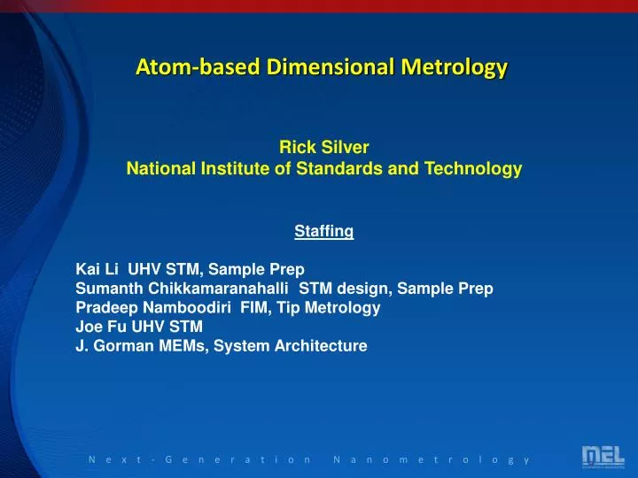
Atom-based Dimensional Metrology. Rick Silver National Institute of Standards and Technology Staffing Kai Li UHV STM, Sample Prep Sumanth Chikkamaranahalli STM design, Sample Prep Pradeep Namboodiri FIM, Tip Metrology Joe Fu UHV STM J. Gorman MEMs, System Architecture.

E N D
Atom-based Dimensional Metrology Rick Silver National Institute of Standards and Technology Staffing Kai Li UHV STM, Sample Prep Sumanth Chikkamaranahalli STM design, Sample Prep Pradeep Namboodiri FIM, Tip Metrology Joe Fu UHV STM J. Gorman MEMs, System Architecture
PED Expertise in the Nanomanufacturing Domain • There is a demonstrated need for standards, metrology, and fabrication techniques to support the growing nanotechnology manufacturing industry. • The semiconductor and high-density memory manufacturing industries have already bridged the gap to high volume manufacturing at the nanometer scale. • PED has extensive expertise in atomically sharp tip fabrication and metrology. • At the forefront of silicon surface preparation methods for atomic resolution imaging. • PED has been a recognized technical leader in atom-based dimensional metrology and nanometer scale fabrication. • DARPA is funding a major thrust to develop the fabrication techniques and metrology methods needed to manufacture at the near atomic domain. • Both industry and university partners in this substantial effort rely on NIST expertise and leadership in several of the key focus areas.
Learning from the Silicon Industry • Process control is the primary challenge. • Feed forward and feed back process control strategies. • Accuracy increasingly important as feature sizes shrink • Metrology tool throughput, cost of ownership. • Resolution versus throughput challenges • Accurate dimensional measurements of 2 and 3-d features. • High-resolution measurement of detailed feature attributes. • Accurate feature placement and overlay in angstroms. • Measuring and understanding materials properties and dimensions at the atomic scale. These current requirements provide good direction and guidance in the future and anticipated needs of nanomanufacturing.
Meeting the needs: Standards and Measurements Standards: • We can anticipate the need for overlay standards, critical dimension standards, materials composition standards. • Standards at the atomic scale are not available. • There are many challenges in the development and fabrication of standards with nanometer scale features. Measurement techniques: • CD measurements with atomic scale resolution. • Feature size and composition • Positioning accuracy of less than a nanometer. • Measurement techniques are needed to link the atomic domain to the macroscopic environment. • Measurement and fabrication techniques with high enough resolution and acceptable throughput remain a challenge.
Primary Technical Challenges • STM tip fabrication and characterization • Goal is robust, repeatable atomic resolution tips. • Daily processing of W and Pt-Ir tips with atomic sharpness. • Sample Preparation • Develop comprehensive process control and calibration for temperature and pressure • Repeatable atomically ordered silicon processing needs to be achieved. • Routine and robust hydrogen terminated surfaces with acceptable levels of surface contamination. • Fabrication techniques • Optimizing patterning and depassivation methods. • Oxidation and epitaxial silicon growth methods. • Need to implement RIE procedures at the atomic scale. • Fiducial mark design and reticle fabrication • Design and robust Si processing for fiducial marks. • Integrating the fabrication and metrology .
500 nm 500 um AC and DC Etch Processes for Various Metallic Tips Etched W(110) tip Omicron W(110) tip • DC etching to obtain the optimum shank shape. Etched W (110) tip Etched Ir tip Etched Pt-Ir tip • AC etching is used to obtain the smallest possible apex radius. • Various etching conditions have been explored to understand the effects on tip shape and sharpness. • The macroscopic tip shape can interact with the atomic apex.
110 121 111 121 110 121 110 W(111) Imaging voltage 1.7kV – 2.6kV ; MCP 1kV; Screen 3.5kV , Base Pressure 3 ×10⁻⁹mbar ; Helium Pressure 1 ×10⁻⁵mbar Temperature ~ -170C Field Ion Microscopy of Metallic Tips • Evaporation Sequence of W(111) trimer producing an atomically sharp tip shown above. • The FIM is used to shape and clean the tip prior to high temperature processing. • We have developed a reproducible high temperature tip process that produces atomic resolution on a daily basis. This represents a major advance.
500 um Evaluation of Different Orientation Etched Tungsten Tips Omicron W(110) tip • Metal Tips for STM Imaging • W (110) Tip (Omicron) • W (111) etched tip • W (110) etched tip • FIM tips until stable emission is observed on the screen • Tip Flashing Procedure • All of the above tips are flash heated using a radiative heater at 935°C • Flash Time: 2 minutes • The thermal processing step is a key to atomic resolution. The University of Texas is now modeling this process to gain a better understanding. • DC etching W (110) etched tip • AC etching, smallest apex
Imaging Evaluation of Etched Pt-Ir, Ir Tips • FIM tips until stable emission is observed on the screen • Tip Flashing Procedure • Ir tips are flash heated at 850 °C • Flash Time: 2 minutes SEM Image of a Ir tip from Custom Probes STM Image using Ir Tip • FIM tips until stable emission is observed on the screen • Tip Flashing Procedure • Pt-Ir tips are flash heated at 650 °C • Flash Time: 2 minutes SEM Image of aEtched Pt-Ir tip STM Image using Pt-Ir Tip Multiple materials have been processed to obtain repeatable atomic resolution images. Note the different tip processing conditions.
Robust Si (100) Sample Preparation Procedures Sample Cleaning Procedures 1. Sample is cleaned using deionized water (18.2 M-cm resistivity) 2. Sample is cleaned using Isopropyl alcohol in an ultrasonic bath 3. RCA cleaning (SC-1 cleaning step) Sample is immersed in a 1:1:5 solution of NH4OH:H2O2:H2O at 75~80ºC for 10 minutes The sample is rinsed in ultrasonic bath using deionized water The sample is immersed in a 1:30 solution of HF:H2O at room temperature for 3 minutes Rinse sample in deionized water and dry with ultra high pure nitrogen gas Annealing Procedures Base pressure inside the UHV chamber: 4 10 -10 torr Degas sample by directly heating it to 600ºC and maintaining temperature overnight Thermally flash the sample from 600ºC to 1100ºC, while making sure that the base pressure inside the UHV chamber does not exceed 1 10 -9 torr. Repeat the procedure until we can hold the sample at this temperature for 20 – 30 seconds. Thermally flash the sample from 600ºC to 1200ºC, while making sure that the base pressure inside the UHV chamber does not exceed 1 10 -9 torr. Repeat the procedure until we can hold the sample at this temperature for more than 30 seconds Once we hold the temperature for more 30 seconds, we cool the sample rapidly to 950ºC and then start cooling the sample slowly at the rate of 1ºC per second.
Repeatable STM Imaging of Si (100) Samples usingHigh Temperature Annealing LEED pattern of the p-doped Si 100 sample after STM imaging Boron (P) Doped Si 100, Flat @ 110, Resistivity: 0.01 – 0.02 cm LEED patterns are used to correlate process and surface conditions with STM images. Used as an average surface indicator. The data above shows the bare silicon surface prior to hydrogen termination. This reconstructed atomic surface is the foundation on which future processes are based. Minimal contamination is also needed.
H2 Passivation Results Using Tungsten Filament Imaging conditions: +2V Bias with 0.4 nA set point current, Ir Tip Imaging conditions: -2V Bias with 0.4 nA set point current, Ir Tip • Very well ordered silicon surfaces are shown here after hydrogen termination. • The images are some of the highest resolution images of the terminated surface obtained to date. • This surface process represents a substantial improvement in repeatable silicon surface preparation. • Passivation Parameters • H2 pressure: 7 × 10⁻⁶ torr, Filament Temp 1450 °C, sample temp: 390 °C, Passivation Time: 10 minutes
Depassivation of H-terminated Si Surfaces Writing Conditions: 4.00V, 2.5 nA to 3.2 nA Writing Conditions: 4.00V, 2.25 nA Writing Conditions: 4.00V, 2.7 nA Writing Conditions: 4.00V, 3.0 nA • Controlled depassivation of the hydrogen termination. • The hydrogen atoms can be removed to expose the reactive underlying silicon surface. This is the key step in atomic resolution directed patterning. • This step is followed by SiO2 hard etch mask formation.
Developing SiO2 Hard Etch Mask RIE Process • Following UHV high temperature atomic surface preparation and h-termination in UHV, the patterns are oxidized. • This forms an SiO2 hard etch mask. • Current work is focused on developing a robust UHV oxidation process. • These processes work must be compatible with fiducial mark stability. • Next, we need to extend the sub-10 nm RIE etch process to the atomic domain. Before and after RIE etching.
Fiducial Structures Fabricated in Si • Designs require two levels of fiducial marks. • Macro marks are 1 to 2 mm in width and 10 to 20 mm in length on a large pitch intended to enable target identification on external metrology tool. • The second level of fiducials are intended to link multiple tips or writing fields in future arrayed tip architectures. • High temperature processing experiments to determine which marks are robust and to processing conditions.
AFM Images of Si (100) surface with fiducial marks • The fiducial marks survived 1200 °Cannealing and are optically visible. Widely spaced marks survive with limited effect on long distance reconstruction. • These marks can be used to influence the surface reconstructions and have become a process design tool. Before Annealing Post Annealing at 1200 °C
30 µm AFM images of an annealed Si (100) sample with Fiducials: Engineering the Atomic Landscape Atomic Scale features are seen in all locations. The example on the right shows double atomic steps . Symmetric step formation seen only on 25µm boxes at 45 degrees angle Topography 3D Topography 3D Topography 3D We have demonstrated that the fiducial pattern and dimensions have a strong effect on the resulting surface.
Conclusions • There are several key applications that will require atomic scale fabrication. • Reticle and master fabrication • Calibration standards • Significant technical progress accomplished • Robust tip preparation • Atomic sample prep • Routine atomic fabrication • A vast array of technical expertise is required to advance both the underlying measurement science and practical applications. • PED has played a central role in the DARPA funded Atomically Precise Manufacturing Program. • Arrayed scanned probes for nanometer-scale metrology measurement systems or fabrication capabilities. • MEMs technologies is enabling rapid progress.