Download
1 / 1
10 likes | 114 Views
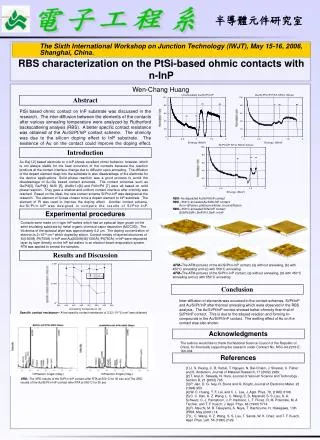
半導體元件研究室. The Sixth International Workshop on Junction Technology (IWJT), May 15-16, 2006, Shanghai, China. Stack-layered metals AuSiNi ohmic contact to n-InP. Wen-Chang Huang, Chih-Chia Wang. Abstract.

E N D
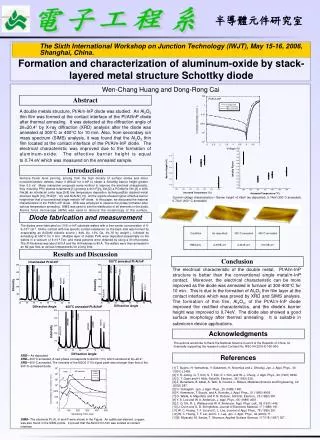
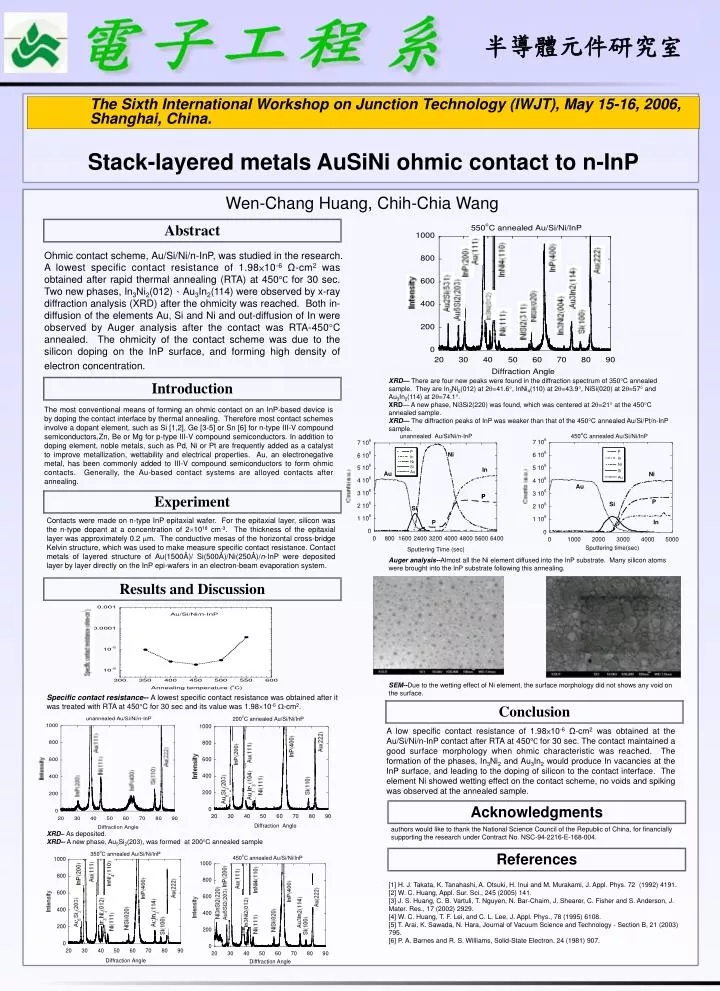
半導體元件研究室 The Sixth International Workshop on Junction Technology (IWJT), May 15-16, 2006, Shanghai, China. Stack-layered metals AuSiNi ohmic contact to n-InP Wen-Chang Huang, Chih-Chia Wang Abstract Ohmiccontact scheme, Au/Si/Ni/n-InP, was studied in the research. A lowest specific contact resistance of 1.98×10⁻⁶ Ω-cm2 was obtained after rapid thermal annealing (RTA) at 450℃ for 30 sec. Two new phases, In3Ni2(012)、Au3In2(114) were observed by x-ray diffraction analysis (XRD) after the ohmicity was reached. Both in-diffusion of the elements Au, Si and Ni and out-diffusion of In were observed by Auger analysis after the contact was RTA-450C annealed. The ohmicity of the contact scheme was due to the silicon doping on the InP surface, and forming high density of electron concentration. XRD— There are four new peaks were found in the diffraction spectrum of 350C annealed sample. They are In3Ni2(012) at 2=41.6, InNi4(110) at 2=43.9, NiSi(020) at 2=57 and Au3In2(114) at 2=74.1. XRD— A new phase, Ni3Si2(220) was found, which was centered at 2=21 at the 450C annealed sample. XRD— The diffraction peaks of InP was weaker than that of the 450C annealed Au/Si/Pt/n-InP sample. Introduction The most conventional means of forming an ohmic contact on an InP-based device is by doping the contact interface by thermal annealing. Therefore most contact schemes involve a dopant element, such as Si [1,2], Ge [3-5] or Sn [6] for n-type III-V compound semiconductors,Zn, Be or Mg for p-type III-V compound semiconductors. In addition to doping element, noble metals, such as Pd, Ni or Pt are frequently added as a catalyst to improve metallization, wettability and electrical properties.Au, an electronegative metal, has been commonly added to III-V compound semiconductors to form ohmic contacts. Generally, the Au-based contact systems are alloyed contacts after annealing. Experiment Contacts were made on n-type InP epitaxial wafer. For the epitaxial layer, silicon was the n-type dopant at a concentration of 21018 cm-3. The thickness of the epitaxial layer was approximately 0.2 m. The conductive mesas of the horizontal cross-bridge Kelvin structure, which was used to make measure specific contact resistance.Contact metals of layered structure of Au(1500Å)/ Si(500Å)/Ni(250Å)/n-InP were deposited layer by layer directly on the InP epi-wafers in an electron-beam evaporation system. Auger analysis--Almost all the Ni element diffused into the InP substrate. Many silicon atoms were brought into the InP substrate following this annealing. Results and Discussion SEM--Due to the wetting effect of Ni element, the surface morphology did not shows any void on the surface. Specific contact resistance-- A lowest specific contact resistance was obtained after it was treated with RTA at 450C for 30 sec and its value was 1.9810-6-cm2. Conclusion A low specific contact resistance of 1.98×10⁻⁶ Ω-cm2 was obtained at the Au/Si/Ni/n-InP contact after RTA at 450℃ for 30 sec. The contact maintained a good surface morphology when ohmic characteristic was reached. The formation of the phases, In3Ni2 and Au3In2 would produce In vacancies at the InP surface, and leading to the doping of silicon to the contact interface. The element Ni showed wetting effect on the contact scheme, no voids and spiking was observed at the annealed sample. Acknowledgments authors would like to thank the National Science Council of the Republic of China, for financially supporting the research under Contract No. NSC-94-2216-E-168-004. XRD– As deposited. XRD-- A new phase, Au5Si2(203), was formed at 200C annealed sample References [1] H. J. Takata, K. Tanahashi, A. Otsuki, H. Inui and M. Murakami, J. Appl. Phys. 72 (1992) 4191. [2] W. C. Huang, Appl. Sur. Sci., 245 (2005) 141. [3] J. S. Huang, C. B. Vartuli, T. Nguyen, N. Bar-Chaim, J. Shearer, C. Fisher and S. Anderson, J. Mater. Res., 17 (2002) 2929. [4] W. C. Huang, T. F. Lei, and C. L. Lee, J. Appl. Phys., 78 (1995) 6108. [5] T. Arai, K. Sawada, N. Hara, Journal of Vacuum Science and Technology - Section B, 21 (2003) 795. [6] P. A. Barnes and R. S. Williams, Solid-State Electron. 24 (1981) 907.