Download
1 / 19
190 likes | 301 Views
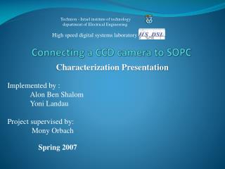
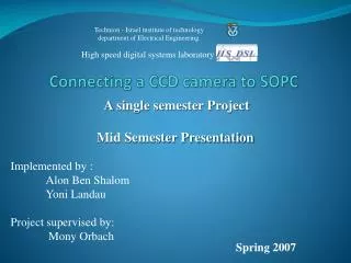
Technion - Israel institute of technology department of Electrical Engineering. Connecting a CCD camera to SOPC. High speed digital systems laboratory. A single semester Project Final Presentation. Implemented by : Alon Ben Shalom Yoni Landau Project supervised by: Mony Orbach.

E N D
Technion - Israel institute of technology department of Electrical Engineering Connecting a CCD camera to SOPC High speed digital systems laboratory A single semester Project Final Presentation Implemented by : Alon Ben Shalom Yoni Landau Project supervised by: Mony Orbach Spring 2007
Agenda • Project Goals • Devices & Environment • Block Diagram • Config Module • Capture Module • Frame capture algorithm • Troubleshooting & Solutions • Conclusions
Adapter Vertex II PRO ov5017 XUP External power supply Project Goals • Capture a single frame through a CCD camera • and forward it to SOPC memory (BRAM) using • Virtex II PRO. • Study VirtexIIpro development environment ( EDK 9.1) • and the design tools ( HDL designer, Modelsim ) CCD Camera
Devices & Enviroment CCD Camera - ¼ ” Monochrome digital camera The M4088 digital camera is based on OV5017 CCD chip manufactured by OmniVision. Chip Interface : M4088 camera module. Development Environment FPGA - Xilinx VirtexIIpro EDK - platform studio 9.1 VHDL code was created using HDL Designer 2007.1 Logic simulation - Modelsim M4088
Devices & Enviroment(Cont.) • Adapter is composed of 2 “Fairchild” buffers
Block Diagram SOPC structure • Module is connected directly to PLB (Max throughput) • CPU, using burst, samples core data and writes it to memory • OCM – CPU’s instruction memory
Core Block Diagram Camera outputs • We need to mux the signals since the high-Z state is not available inside the VERTEX IP. • Muxed signals are connected to the same connectors Data Config MUX FPGA inputs Camera outputs Address,OEB,CSB,WEB Capture Camera inputs FPGA output Data,ready
Config Module In order to get a frame there’s a need to configure the camera to user needs. It’s done by writing to a specific register in camera at address “0101”. The following figure illustrates a single byte write to a specific register.
Config Module (Cont.) The user configure the camera through C code. Data is delivered to the Config Module by the CPU, when start signal rise to ‘1’ the module sets The relevant data to camera and the configuration is implemented. The module is a state machine setting the data to camera
From C command to Module • 32 bit registers were allocated by EDK • Data is transferred from C code through the registers to Modules • No need to recompile HW whenever data changes • C code to Module interaction example
Capture Module After the user configured the camera he sets start to ‘1’ (through C Code) , the module starts setting the outputs to camera so the frame data is Received from camera. Frame is composed of 384*288 pixels (pixel is a byte) The following figure illustrates a frame data stream – It’s actually reading A data register
controller FIFO outputs inputs coordinator Shift register Capture Module (Cont.) The Module is composed of several sub modules interacting with each other in Order to synchronize FPGA with camera.
controller FIFO outputs inputs coordinator Shift register Capture Module – Behavioral Description • Start rise to ‘1’ – Controller sets the Camera to data stream. When a new frame starts controller send “in_win” signal to shift Register for start storing data and send it to FIFO • Shift register counts 4 pixels (pixel=byte), it converts The 4 bytes to a 32 bits word and send a “ready” signal to FIFO • FIFO accumulates 8 words (32 bits each), when finished It sends “all_ready” signal to coordinator, which in response raises the “all_reg_trig” signal to FIFO in order to move the 8 words to the second level in the FIFO and signal to the CPU to start reading. Coordinator waits for the CPU to write the Data to memory, when CPU finishes it sends to the Coordinator ACK signal
Frame capture algorithm The following diagram illustrates the stages of a frame capture
Troubleshooting & Solutions • Module was originally connected to OPB - CPU didn’t succeed writing data to memory on time due to the fact it should go over the PLB/OPB bridge (Real time system complication) • Module was moved to PLB
Troubleshooting & Solutions - Cont’d • CPU instruction memory was connected to PLB – Bus is very active • Instruction memory was replaced by OCM – Low competition over the PLB resource
Troubleshooting & Solutions - Cont’d • Read/Write bus access was too slow for data rate • Using Read/Write burst bus access to improve throughput • Unreliable synchronization signal behavior of camera • Logic solution (debouncer) • Voltage mismatch between camera to FGPA connectors • We built an adapter to resolve this issue
Conclusions • A better solution for capturing a frame could be moving the data using DMA. This way there were much less bus transactions, therefore a much faster solution.