Download
1 / 20
211 likes | 390 Views
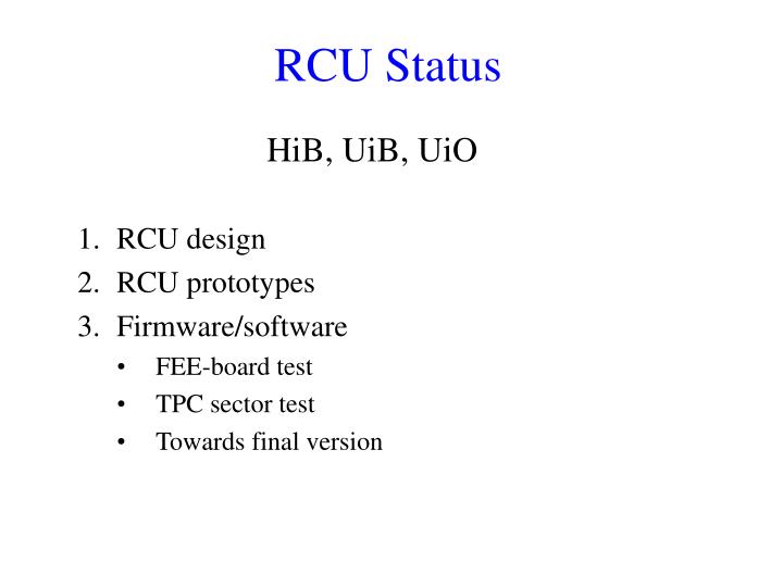
RCU Status. HiB, UiB, UiO. RCU design RCU prototypes Firmware/software FEE-board test TPC sector test Towards final version. 1. RCU design – control flow. TTCrx. SIU controller. FEE bus controller. State machines. DDL command decoder. FEE SC. RCU resource &

E N D
RCU Status HiB, UiB, UiO • RCU design • RCU prototypes • Firmware/software • FEE-board test • TPC sector test • Towards final version
1. RCU design – control flow TTCrx SIU controller FEE bus controller • State machines DDL command decoder FEE SC RCU resource & priority manager Huffman encoder DCS low level Watchdog 2 Watchdog 1: health agent Debugger DCS high level PCI core
RCU design - data flow • Shared memory modules TTC controller TTCrx registers FEE bus controller Event memory 1 Event memory 2 SIU controller fifo FEE bus controller Event fragment pointer list SIU Huffman encoder FEE bus controller Configuration memory DCS
2. RCU prototypes • Prototype I • Commercial OEM-PCI board • FEE-board test (ALTRO + FEE bus) • SIU integration • Qtr 3, 2001 – Qtr 2(3), 2002 • Prototype II • Custom design • All functional blocks • PCB: Qtr 2, 2002 • Implementation of basic functionality (FEE-board-> SIU): Qtr 3, 2002 • Implementation of essential functionality: Qtr 2, 2003 • (Prototype III) • SRAM FPGA -> masked version or Antifuse FPGA (if needed) • RCU production • Qtr 2, 2003
RCU prototype II • Implementation of essential functionality • Custom design • All functional blocks DCS FEE-bus DCS TTC rx FEE-bus FEE SC PCI bus PCI core FPGA SIU internal SRAM SIU-CMC interface > 8 MB FLASH EEPROM Memory D32
RCU prototype II - layout • Motherboard • FPGA • memory data buffer • memory work space • ethernet • PCI interface • CMC connectors • Mezzanine card I • SIU • Mezzanine card II • FEE bus A and B • TTCrx • Profibus interface
JN2A JN1 JN2 Flash Power (1.8V Gen.) Flash Flash SRAM SRAM SRAM SRAM JN3 JN4 JN5 APEX SRAM SRAM SRAM SRAM Connectors SDRAM RCU prototype II - motherboard
Front-End Bus Conn 1 RCU Mezzanine Card Components on top side No maximum height restriction Front-End Bus Conn 2 RCU prototype II – mezzanine cards SIU mezzanine card (1/2 CMC)
RCU prototype II - status • Floor plan of PCI board • Status motherboard (in collab. with HD) • design and layout done • PCB production in May • mounting of components in May/June • testing debugging 107 mm 314 mm
RCU prototype II - status • Status mezzanine boards • SIU (needs adapter) • FEE-bus, TTCrx, Profibus • design done • layout and PCB production in May
RCU prototype II - status • TTCrx
RCU prototype II - status • Profibus
RCU prototype II - status • FEE-bus • two branches • external multiplexing • internal (inside FPGA) multiplexing (modified mezzanine board)
3. Firmware/software – status and plans • Test environment for FEE-boards • TPC sector test • Towards the final version
FEE test environment GUI? • Application program: • C/C++ • GUI? PC LINUX RH7.2 RCU/ALTRO test tool RCU-API • ”Special RCU”: not TTCrx, no DCS, no SIU device driver PCI core mailbox memory PCI FPGA board FEE bus controller tester FEE bus Signal generator FEE-board (ALTRO)
RCU system for TPC test 2002/2003 • Readout of 4 FEE-bus branches • 2 RCU prototypes II • fallback solution: 4 (2) RCU prototypes I (3 boards are available) • Basic RCU functionality • configure FEE (done) • readout event (being debugged) • develop logics for readout of all FEE cards on FEE-bus (design in progress) • include external SRAM (designed, simulated, being tested) • develop RPM for controlling data transfer from FEE-bus to SIU (design started) • Include simple trigger and event-ID • Interface to DATE • DAQ via DDL • 2 pRORC (including SIU + DIU) • Integration of pRORC: DATE 4 (June 2002) • fallback solution: DAQ via RCU-PCI
FEE-boards RCU system for TPC test 2002/2003 RCU prototype II/I Trigger FEE-bus LINUX RH7.2 FEE configurator PLDA/PCI-tools RCU-API device driver SIU FPGA interface FEE-bus controller SIU controller Manager PCI core SIU SRAM FLASH ext. SRAM PCI bus DDL pRORC DIU LINUX RH7.2 DATE 4 DDL/PCI-tools pRORC-API device driver Glue logic PCI bridge interface DIU PCI bus
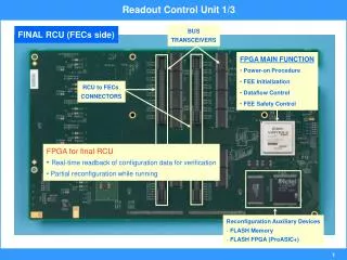
Towards the final version • Radiation induced corruption of SRAM • SEE in configuration SRAM of FPGA will happen • monitor system state and detect such effects -> reset FPGA • two watchdogs • FPGA self-detection • detection by Profibus slave ASIC • DCS • two level interface • Profibus slave controller (ASIC) • ethernet chip • Trigger • one TTCrx per RCU