Download
1 / 19
190 likes | 347 Views
Firmware for the CPLD on the RCU. Kjetil Ullaland, Ketil Røed, Bjørn Pommeresche, Johan Alme. TPC Electronics meeting. CERN 13-14. Jan 2005. Overview. Requirements Concepts of configuration Proposed design Modules RCU bus interface SelectMap interface Flash interface

E N D
Firmware for the CPLD on the RCU Kjetil Ullaland, Ketil Røed, Bjørn Pommeresche, Johan Alme TPC Electronics meeting. CERN 13-14. Jan 2005
Overview • Requirements • Concepts of configuration • Proposed design • Modules • RCU bus interface • SelectMap interface • Flash interface • Readback and verification module • JTAG input block • CPLD • Status
Requirements • Configure the Virtex-II on power-up • Scrubbing of the Virtex-II from Flash • Write configuration-files to the Flash from the DCS-card • Readback and verify configuration memory in Virtex-II with stored files in Flash. • Configure Virtex-II from DCS-card. • Configure the CPLD firmware • Status registers in the CPLD for Config-status, verification etc. • Possibility to load data into flash memory when DCS board is detached.
Concepts of Configuration • A mode register to choose different concepts of configuration (in memory mapped mode): • 0: Scrub At Will • 1: Continously Scrubbing • 2: readback/verify • 3: Clear config memory and configure. • 4: read flash • 5: read config memory • Transport data interface: • Write configuration files to flash • Read configuration files from flash • Write configuration to Virtex-II • Read configuration from Virtex-II • JTAG line to be able to configure Flash.
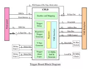
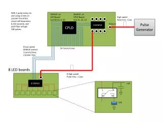
Proposed Design (2) • Two bus modes between DCS and CPLD • Transport data interface. For configuration data streams. • Normal mode. Memory mapped interface for status and control. • Both modes using RCU bus lines. • One control line (DCS_ctrl[7]) is used to switch between the different modes.
Mem mapped mode vs transport data IF Memory mapped mode Fast mode
CPLD Register Map – Mem mapped mode • Status register: • Readback/verification errors (4 bit) • Scrub error (1 bit) • Config error (1 bit) • Flash Communication error (1 bit) • Control register: • Mode of operation (3 bit) • StartScrub • WDMaxValue – Watch dog max value • ScrubRate – Time between each scrub cycle in scrubmode. • FlashBank – Possibility to choose bank in flash where configuration file is. • selMapData – Data to/from the selectMap interface • flashData – Data to/from the flash
Error handling • Watchdog • If Virtex-II doesn’t give a life-pulse within a user-defined time, a complete reconfiguring including clearing of configuratiopn memory is done (hard reset) • Timeout of bus communication • If a write cycle fail on the RCU bus lines, go to default mode • Automatic scrubbing if readback/verification error.
RCU bus interface (memory mapped mode) • Standard memory mapped interface with timeout functionality on bus communication. • Use RCU bus lines between DCS and CPLD.
Transport data interface • Use RCU bus lines between DCS and CPLD.
Selectmap interface • Communicates with the Virtex-II over the selectMap bus. • Complete configuring cycle with non-continuous clock shown.
Selectmap interface • Receives data from two sources: • 32 bits of data from the DCS board • 16 bits of data from the Flash memory interface. • Data must be bitswapped byte by byte. (bin or bit file is used.) • Ships data to two data sources • DCS board, 32 bit at the time • Readback and verification module, 8 bit at the time
Flash interface • Read or write data from/to the flash memory over the dedicated bus. • 16 bit data • 22 bit address • 5 control lines • 3 files must be stored in flash • Bin-file (or bit-file). Configuration data file. • Rbb-file. File used for readback and verification. Copy of the bitstream. • Msk-file. File used for readback and verification. Mask out bits that should not be compared between the rbb-file and the readback bitstream. • All files are approx 368 KB
Readback and verification module • Compares the bitstream from selectMap interface with the rbb-file and msk-file in the flash. RBB[i] = MSK[i] x DATA[i] • If error is found, a scrubbing cycle is initiated immidiately, and the error counter is updated.
JTAG input block • Translates information from the JTAG input and ships it to the Flash interface to write bin-file to the flash.
Choice of CPLD • Configuration memory must be flash based. • Approx max Size (registers): • Registermap 75 • statemachines 32 • addr latch 4 • data latch 32 • wd cnt 30 • scrubrate cnt 30 • Flash addr cnt 44 • Timeout cnt 4 • Synchronizers 3 • Framecounters 20 • SUM ~300 • One register per macrocell means we need at least 300 macrocells.
Status • Preliminary specifications are finished. • Some issues need further investigation. • Readback and verification • Partial reconfiguration