Download
1 / 39
410 likes | 527 Views
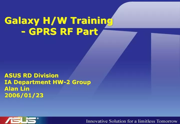
Galaxy H/W Training - GPRS RF Part ASUS RD Division IA Department HW-2 Group Alan Lin 2006/01/23. Agenda. Introduce to GPRS Function - Block Diagram - Key Parts List - Aero II Architecture Highlights - Transmitter - Receiver Trouble Shooting - Ckt. & Location - AFC - APC

E N D
Galaxy H/W Training - GPRS RF PartASUS RD DivisionIA Department HW-2 GroupAlan Lin2006/01/23
Agenda • Introduce to GPRS Function • - Block Diagram • - Key Parts List • - Aero II Architecture Highlights • - Transmitter • - Receiver • Trouble Shooting • - Ckt. & Location • - AFC • - APC • - AGC
PMIC Analog IQ T/R SW RF Chip BB Chip Flash BB Part PA RF Part FFUART Pink : GPRS RF Green : GPRS Base-Band Blue : PDA PDA Part GPRS Block Diagram
Transceiver Block Diagram 1800: 856409 1900: 856417 850: 856441 900: 856387 LMSP33QA-321 RF3166
Audio RX path Analog IQ signal Audio TX path 3 wire bus for RF transceiver SIM RF Control T/R switch Base-band Block Diagram
Aero II RX Highlights • Low IF architecture strengths (200kHz IF) • Has advantages of Super-Heterodyne architectures : • DC Offsets are located outside the band of interest. • IP2 (AM Suppression) requirements are relaxed. • LO Self Mixing is not a problem. • Has advantages of Direct Conversion architectures : • No IF SAW Filter required – Image Rejection requirements are simplified. • Single analog down-conversion stage. • IF Analog Signal Processing is at a low frequency. • Digital IF signal processing.
Transceiver Functional Block Universal Baseband Interface (DAC) RX Loop RX SAW TX Loop Power Amp. Synthesizer XTAL(DCXO)
Receiver Block Diagram Image Reject Low - IF Receiver
Aero II TX Highlights • Offset PLL architecture • Band Pass Noise Transfer Function attenuates noise in RX band. • TXVCO is a constant-envelope signal that reduces the problem of spectral spreading caused by non-linearity in the PA. • Eliminates need for TX SAW Filter. • TX transmit out buffer • Helps eliminate spurs and pulling issues.
Transmitter Block Diagram Offset PLL
Advantage - Low noise floor and spurs - Pulling of the transmit VCO is reduced -Truly constant envelope Output from VCO Offset PLL • The OPLL acts as a tracking band-pass filter tuned to the • desired channel frequency. • The important difference between a PLL and the OPLL is • that the frequency modulation of the reference input is • reproduced at the output of the Tx-VCO without scaling • Disadvantage • - Only possible with constant envelope modulation scheme
DCXO Architecture Frequency adjusted by two variable capacitances - Cdac: coarse tuning - Cafc: fine tuning
Phone Tool GSM tester Data cable Spectrum Analyzer RF adaptor RF I Q DUT Oscilloscope Measurement Equipment • Agilent 8960 / CMU200 • Power Supply • Scope • Spectrum • Passive Probe with DC Block
Base Station Setup • Base Station Test Mode Setup
Antenna Switch Connector Antenna Switch Connector Bottom Side
Low band Matching PA PA & Front-end Top Side T/R Switch High band Matching
PA & Front-end PALEVEL (VRAMP) Low band Matching PA High band Matching T/R Switching
RX Path Top Side XTAL Transceiver RX SAW T/R Switch
RX Path T/R Switching RX SAW Transceiver RX SAW XTAL
Trouble Shooting • AFC Fail • APC Fail • AGC Fail • ORFS due to Modulation Fail @ -200kHz & +400kHz fail • Others
AFC & TX Testing Nodes B A E F G C D H
AFC Fail • Check antenna switch connector • Check Vramp & PA output power • Check 26MHz output PA
T/R SW High-band out Low-band out Low-band in High-band in Vramp APC Fail • If TX current is right - Check antenna switch connector - Check T/R switch - Check PA matching circuit
T/R SW High-band out Low-band out Low-band in High-band in Vramp APC Fail • If TX current is small - Check TXVCO output - Check Vramp - Check PA - Check VBAT
26MHz & TXIQ Fig. 1.2 TXIQ Fig. 1.1 26MHz
TXVCO Fig. 1.3 TXVCO DCS Ch700 : 1747.8MHz Fig. 1.4 PA Out DCS Ch700 : 1747.8MHz
Vramp Fig. 1.5 Vramp
RX Testing Nodes F A E B D C
AGC Fail • Check antenna switch connector • Check T/R switch • Check SAW • Check RXIQ RX SAW
26MHz & T/R Switch Out Fig. 2.1 26MHz Fig. 2.2 EGSM Ch62 : 947.4MHz
RX IQ Fig. 2.5 RX IQ