Download
1 / 16
160 likes | 356 Views
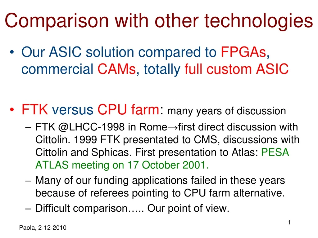
Comparison with other technologies. Our ASIC solution compared to FPGAs , commercial CAMs , totally full custom ASIC FTK versus CPU farm : many years of discussion

E N D
Comparison with other technologies • Our ASIC solution compared to FPGAs, commercial CAMs, totally full custom ASIC • FTK versus CPU farm: many years of discussion • FTK @LHCC-1998 in Rome→first direct discussion with Cittolin. 1999 FTK presentated to CMS, discussions with Cittolin and Sphicas. First presentation to Atlas: PESA ATLAS meeting on 17 October 2001. • Many of our funding applications failed in these years because of referees pointing to CPU farm alternative. • Difficult comparison….. Our point of view.
Comparison AMchip – other technologies http://www.pi.infn.it/%7Eorso/ftk/53tns04-giannetti-pt2-proof.pdf For a comparison of standard cell Amchip, Full custom, FPGAs & commercial CAMs solutions The AMchip History – the idea is born in 1985 • 1990 Full custom 700 nm: 128 pat/chip, 1 pattern = 6 layers x12 bit F.Morsaniet al., IEEE Trans. on Nucl. Sci., vol. 39, pp. 795-797 (1992) advantages: pattern density problems: not possible to simulate intensively the logic; hard to upgrade • 1996 FPGA 350 nm: 128 pat/chip, 1 pattern = 6 layers x12 bit P.Giannettiet al., Nucl. Intsr. and Meth., vol. A413/23, pp.367-373, (1998) advantages: easy design and debugging, full simulation available problems: low pattern density, cost, difficult package selection, not pin-compatible evolution, unexpected, problematic changes due to market. • 2004 Standard Cell 180 nm: 5 kpat/chip, 1 pattern = 6 layers x18 bits A. Annoviet al., IEEE Trans. on Nucl. Sci., vol. 53, pp.: 2428 – 2433 advantages: easy design, full simulation available,…. Ithas the advantagesof FPGAs without sharing its problems. Lower pattern density than full custom.
Empty SSs The FPGA AM project for the RW We have used FPGAs for low density AMs in the Road Worrior design: IEEE TNS Volume: 53, Page(s): 648 - 652 (2006) There patterns are simply coded in registers: 15 x8= 120 bits = 120 FFs RW works on SS before knowing the fit chi**2 It deletes ghosts acting on roads that differ for a single empty SS RW reduces fits to be done Paola TDAQ 15-05-2008
The FPGA AM project for the HW And we propose their use in the FTK Hit Warrior function: Technical Proposal pag. 41, same style of NIM, vol. A413/23, pp.367-373, (1998) There patterns are coded in LUTs exploiting carry chains
How many patterns we could fit in modern FPGAs? The present: choice based on cost and package: XC6SLX150T-4CSG484 (19x19 mm^2) 4 GTPs 296 pins (our package is LQFP208) 373 $ today → 16400 AMchips → 6 M$ 23 k slices, even assuming ~8 slices/pattern → ~2.9 k patterns/FPGA <<< 80 kpat/(our Amchip: 12x12 mm^2 65 nm) The future http://www.xilinx.com/technology/roadmap/7-series-fpgas.htm Best Virtex 7 XC7V200T (new family not available now) 305 k slices → ~ 38 kpatterns/FPGA < 80 kpat/(our Amchip) Using FFs: 2,443 Mff → ~120 FF/pattern → ~ 20,4 kpat/FPGA Even using Slices and FFs together < 80 kpat/(our Amchip) Even choosing thebest device of next years Even if we don’t care about cost and package Even with veryoptimistic hypothesison a difficult design we don’t get our AMchippower!
One single large word (up to 576 bits) where each SS in all the layers is counted has 1 (set), 0 (not set) or X (don’t care). Wait all detector wedge readout to build this long word for each event, than compare in a single clock L2 L1 SS encoded in 15 bit words L2: too many SS to fit in 576 bits! L1: latency to build the large word sent only at the end of event!
Our chip today and its evolution • Today: a 2D chip with two standard cells designed by us: (a) pattern & (b) majority + TSMC standard cells for control logic • For Phase II (after 2020): a 3D chip Two possible Approaches to expand into the third direction VIPRAM - Vertically Integrated Pattern Recognition Associative Memory Ted, Jim, Aida, Ray, Gregory, Simon, Silvia, Marcel, Gary, Mel, Bob • FNAL/ANL/UC/Tezzaron/… • “Identical Tier” 3D architecture (actually 2.5 D?) • “True 3D” Implementation
HOW to do a 2.5 D chip starting from a 2 D device? • The 3D IO Wrapper must be designed and fabricated around the 2D AMchip to ensure that all tiers act as a single chip as shown in Figure 5. • Even for prototyping purpose, it is not possible to simply take an existing, fabricated AMchip and place it inside a rectangular doughnut-shaped 3D IO Wrapper. There are several ways to address this. • First, the 2D AMchip could be redesigned in a 3D process like Tezzaron/Chartered, and then the 3D IO Wrapper could be designed around it. This method has no obstacles to its 3D fabrication. However, it does require the redesign of the AMchip. • Second, the CMOS TSMC process could be used for 3D development even though TSMC does not have a 3D process. This method requires no redesign of the AMchip, but it does require TSMC to be willing to participate in a “Via Middle” process in which after a certain number of fabrication steps, the wafers are shipped to a “Via Middle company” (e.g. Tezzaron) where the first steps of the Through Silicon Via process are started. Then the wafers are shipped back to UMC where the 2D processing is completed. Finally, UMC ships the completed wafers to the Via Middle Company where 3D processing is completed. Not all companies are willing to participate in a Via Middle process.
The True 3D: 1 tier/ Layer +1 control tier Control Tier Tier 4 Tier 3 Tier 2 Tier 1
CPUs vs FTK: some important # for Phase I • The complexity of events is extreme: running on WH events with 75 pile-up events we find an average number of 40 jets with Pt above 70 GeV (we are the first users of the simulation @ high pile-up, the package is probably not optimized). ROI search LOOKS similar to full event reconstruction. • FTK finds all trakcs > 1 GeV Pt at 100 kHz event rate in a average latency time of 25 ms to leave all the remaing time to high quality algorithms. Is it important to have the tracking job made in a short latency? How much short should be? • Is it important to have all event tracks reconstructed with a short latency? How much short should be? Let’s suppose we all agree that it is important to have the FTK job done in a very short time.
Timing: Simulatiom of FTK & CPU system for WH +75 pile-up events • Timing studies with 75 pile-up events (see Mel slides) → FTK much better than standard CPUs working on jet ROIs. • What about a CPU specific architecture for tracking (GPUs?) ? Could be competitive? We don’t know. We need a GPU expert group to evaluate it. • Difficult work, takes time… cannot be done by us. • BUT, if in six years from now we need the FTK job, we have to start now to work hard, in both cases FTK-FPGA like or FTK-CPU like.
FTK-FPGA like Computing Power: [ 324 (DF) + 256 (AMBoards) + 1152 (AUX Boards) + 128 (Final Boards)]FPGAs = 1860specialized FPGAs + 16400 AMchips working in pipeline (each stage ~ 10 ms in avearge) with thousands of specialized links! Suppose you could get the FTK 3 M €: can you by ~6 k CPUs ? Are they enough Computing Power? how you divide the tasks and connect them to get a low latency? 128 AMB : 256 FPGAs + 128x128 AMchips Clustering in parallel – 224 clustering FPGAs 48 DF: cross-point for clusters - ~100 FPGAs HOW FTK DOES this JOB ? A pipeline of thousands of dedicated CPUs P3:16x128 serial Links 2-3 GHz each 8 224 Rols 8 32 Final boards: ~128 FPGAs 128x4 DO: ~128x4 FPGAs 128x4 TF: ~128x4 FPGAs 128 HW: ~128 FPGAs Board-board Connector 128x12 fibers Into 128 SNAP12 ~25 ms latency in average 2-3 GHz Each fiber
All technologies do scale with time • CPUs can increase their power in the next years, but also FPGAs and ASIC technologies improves as well, probably more. FPGAs are moving to 3-D organization (stacked silicon interconnect technology). We also are planning to move to 3-D for AMchips for phase II. Can we assert that CPUs evolution will be such to gain in comparison to FPGAs and ASICs in the future? I suspect it is the opposite • Upgrade and maintenance of FTK (12 crates and 4 racks) is not necessarily more difficult than what requires a 6 kCPU farm. • Certainly space, power consumptionis smaller than what necessary for 6k CPU farm, provided 6k CPUs can do the job. • Comparison should include“hardware potentiality” + “team of experts” that wants to implement the project +“funds available to the team”. Two teams present their options. We cannot present both options we are not equally experts of both and we are not the group that would implement the second. We miss informations
Conclusions • The AMchip technology we have chosen comes from our past experience. • The new LHC schedule + “variable resolution pattern” results favor (a) a new 65 nm AMchip implementing the don’t care feature already in 2013, (b) a new 3D AMchip for 2021 (above 40 pile-up events) • FTK versus Farm of CPUs: we can’t exclude that someone else could succeed to do the FTK job with CPUs, but we do not imagine how. Someone more expert than us is needed.