Download
1 / 14
150 likes | 281 Views
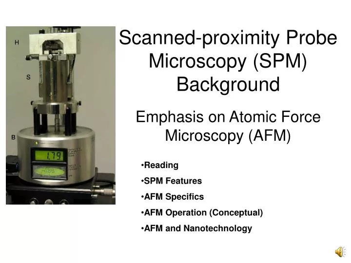
Scanned-proximity Probe Microscopy (SPM) Background. Emphasis on Atomic Force Microscopy (AFM). Reading SPM Features AFM Specifics AFM Operation (Conceptual) AFM and Nanotechnology. Reading.

E N D
Scanned-proximity Probe Microscopy (SPM) Background Emphasis on Atomic Force Microscopy (AFM) • Reading • SPM Features • AFM Specifics • AFM Operation (Conceptual) • AFM and Nanotechnology
Reading • “Window on a Small World,” McGuire, Today’s Chemist, June 2002Vol. 11, No. 5 pp 21–24 http://pubs.acs.org/subscribe/journals/tcaw/11/i06/html/06inst.html • “AFM Technology Overview” From Veeco (Digital Instruments) the manufacturer of the AFM that will be used. • http://nano.nd.edu/SC190/scanningprobe.pdf “AFM Nanomanipulation” From Veeco on the use of the AFM in direct nanotechnology applications. http://www.veeco.com/pdfs.php/70 • Scanning Probe Microscopy (SPM) Instructions http://frontpage.okstate.edu/nanotech/Lab/lab3/SPM_Instructions_082003.pdf
Scanned Proximity Probe Microscopy Common Features • Piezoelectric (PZ) positioning • PZ crystals expand/contract under applied voltage (d11≈ 4x10⁻¹⁰ m/V) • Example: A commercial linear actuator produces 15 mm displacement for 100 V applied with sub nm resolution • PZ crystals generate voltages under applied force (g33≈ 1x10⁻² V/Nm) • Deflection Feedback Loop • Height (z) dependent signal • Example: Tunneling current for Scanning Tunneling Microscope (STM) • Example: Van der Waals forces for Atomic Force Microscope (AFM) • Probe/Tip • Photolithographic Fabrication Techniques • Resolution determined by probe size (not diffraction)
AFM Capabilities (Advantages) • Able to achieve a resolution of 10 pm with special tips (typical resolution ≈ 10 nm) • Able to image samples in air and under liquids • Able to measure in 3 D (within limits) • Able to measure non-conductive surface (unlike SEM or STM)
AFM Capabilities (Disadvantages) • Incorrect tip choice can lead to measurement artifacts or sample damage • Depth of field limited by cantilever / z positioning PZ • Scan area limited by PZ scanners • Slow scan rate compared to SEM
Position Sensitive Photodetector (PSPD) Laser Optical Beam Z Piezoelectric Positioning/ Force Sensor Sample Probe Tip Substrate Cantilever X-Y Piezoelectric Positioning/ Scanning AFM Components
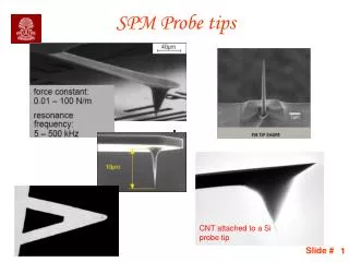
AFM Probe • Tip • Modifies measurements • Typically Si or SiN for ease of fabrication • Many variations depending on application • Cantilever (Tip at the end) • Low spring constant (Hooke’s Law F = -kz) • Low weight for high resonant frequency ( ) • Coated for reflectivity Tip on apex of cantilever Images from http://stm2.nrl.navy.mil/how-afm/how-afm.html#General%20concept
AFM Modes • Contact mode (Repulsive-Static) • AFM tip rides on the sample in close contact with the sample surface (low k) • The force in the feedback loop is friction • May interact with the sample surface • Non-contact mode (Attractive-Dynamic) • AFM tip hovers 5-15 nm away from the sample surface • The force in the feedback loop is typically van der Waals (VDW) forces • Applied force (dependent on height z) changes cantilever oscillation frequency. • Tapping mode (Repulsive-Dynamic) • AFM tip taps surface as it maps z. • Eliminates lateral forces or hysteresis due to the tip sticking on the sample. • Less likely to damage the sample
AFM Measurement Changes of the surface properties along the scan line Changes of interaction forces between the probe tip and sample surface Contact Mode Non-Contact Mode Deflection of the cantilever Change of oscillation amplitude and phase of the cantilever Laser beam position oscillates on the PSPD Change in laser position on PSPD Electronic signal to control and recording electronics Signal processing to form image
AFM Visualization (Contact Mode) PSPD measures change optical beam position change in cantilever height Sample is raster scanned
Forces at Work • Atomic Forces (approx.) U Repulsive Attractive B and A coefficients depend on the surfaces involved. Detectable forces for an AFM 1 nN in the contact regime and 1 pN in the noncontact regime (Theoretical Limit 10-18 N with heroic measures.) R. Wiesendanger, "Chapter 11. Future Nanosensors." In H. Meixner, R. Jones, eds., Volume 8: Micro- and Nanosensor Technology / Trends in Sensor Markets. In W. Gopel, J. Hesse, J.N. Zemel, eds., Sensors: A Comprehensive Survey, VCH Verlagsgesellschaft mbH, Weinheim Germany, 1995; pp. 337-356.
Approach-Retract Phenomenon Approach Snap On Impress Force (proportional to cantilever deflection) Retract Snap Off (NOT the tip Z position!) • Approach—VDW forces pull tip toward surface • Snap On—When close enough, VDW grow stronger than restoring spring force in the cantilever. • Impress—Tip pressed into sample with positive force after reaching the set point deflection • Retract—Tip adheres to surface giving rise to hysteresis on measured force/position curve • Snap Off—Spring force dominates the tip-sample adhesion and tip leaves surface
Alternate Scanning Probe Systems • Magnetic Force—Maps surface magnetic field (think hard drives…) • Electrostatic Force—Maps surface potential (100 nm resolution) • Lateral Force—Maps friction force experienced by scanning probe on surface orthogonal to scanning direction • Magnetic Resonance—Possible 3D imaging of individual molecules via resonant electron spin flipping with an antenna on the cantilever • Near Field Optical Microscopy • Probe tip has a small aperture (radius << l) for optical wavelength measurements • And many, many more…
Nanotech Applications • Measurement of nanostructures • Nano indention of surfaces • Dip Pen Nanolithography • Manipulating nanoparticles (building nanostructures) • Precision electro chemistry—supply electrons by applying voltage across AFM tip and substrate