Download
1 / 22
220 likes | 415 Views
MIPP TDC Card. Wu, Jinyuan Fermilab, PPD/EED Apr. 2007. The TDC Card. MIPP_TDC FPGA. 96 Channels. 12 connectors, 8ch each. Each MIPP_TDC FPGA digitize 48 channels inputs. The MIPP_DCC FPGA concentrate data from two TDC FPGA devices. Up to 32K event/spill are stored in the SDRAM.

E N D
MIPP TDC Card Wu, Jinyuan Fermilab, PPD/EED Apr. 2007
The TDC Card MIPP_TDC FPGA • 96 Channels. • 12 connectors, 8ch each. • Each MIPP_TDC FPGA digitize 48 channels inputs. • The MIPP_DCC FPGA concentrate data from two TDC FPGA devices. • Up to 32K event/spill are stored in the SDRAM. • TDC resolution: 1.18ns (LSB). Bench tested @ 0.69ns (LSB) (See next pages) SDRAM MIPP_DCC FPGA RJ-45 MIPP_TDC FPGA
Clock Domain Changing TDC Inside FPGA Multiple Sampling Q3 QF • Sampling rate: 360 MHz x4 phases = 1.44 GHz. • LSB = 0.69 ns. • Logic elements with critical timing are assigned as shown. c0 c0 QE Q2 c90 QD Q1 c180 Q0 c90 c270 DV T0 T1 Trans. Detection & Encode 4Ch Coarse Time Counter TS Logic elements with non-critical timing are freely placed by the fitter of the compiler.
Bench Test of TDC RAM Flash RAM FPGA eZ80 TDC 45MHz Micro-processor address line driven by 45 MHz clock. 32 TDC bin = 1 clock cycle (0.69ns LSB) RAM Flash RAM FPGA eZ80 TDC 45MHz Micro-processor data line. Data out from different sources.
The FPGA TDC Test Card Shown here is Fermilab Beam Loss Monitor (BLM) Control Card VME Interface (As hit input) FPGA Serial Port Microprocessor
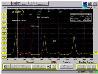
Differential Nonlinearity FPGA Quasi-random Input TDC The “beat” between input and 45MHz. 45MHz The placement above gives even bin width. Occupancy for each bin should 25%. The residual DNL < 690*(26-22)/25 = 110ps
TDC Data Concentration Substituting Multiple Error Sources with Single Error Source
TDC With Hit Rate Limiter 0 1 2 3 4 5 6 7 8 9 a b c Reset 1.2us Counter CC[5..2] TDC T1 T0 DV TDC/HRL DVLD CLR TDC/HRL CK212 L/S Hit Rate Limiter (4/256CK212) TDC/HRL LD CLRHIT LD TDC/HRL CLRCNT 4hits/256CK212, 4hits/1.2ms 3.3MHz
TDC Data Concentration 96 Ch TDC/HRL TDC/HRL Zero Supp. L1 Buffer 1xM4K 16x256 TDC/HRL TDC/HRL Ch 4-7, TDC & L1 Buffer SDRAM 16x8M/spill 16MB/spill Ch 8-11, TDC & L1 Buffer Ch 12-15, TDC & L1 Buffer TDC/L1 Buffer/MUX Channels 16-31 EV Buffer & Truncating 16x128x2 FPGA (DCC) TDC/L1 Buffer/MUX Channels 32-47 EV Buffer & Truncating 16x128x2
Readout Timing 1.2us 0 1 2 3 4 5 6 7 8 9 a b c WR 0,1 0,1 0,1 6.6us RD G0 B=0 G0 B=1 G4 B=0 G4 B=1 G8 B=0 G8 B=1 G12 B=0 G12 B=1 G16 B=0 G16 B=1 G20 B=0 G20 B=1 G24 B=0 G24 B=1 G28 B=0 G28 B=1 G32 B=0 G32 B=1 G44 B=1 1.2us
17 16 15 14 13 12 11 10 9 8 7 6 5 4 3 2 1 0 Data Format 0 0 0 No Data 1 0 0 EHID[5..0] CNT[7..0] P EV Header 0 1 0 0 EV[13..0]=1, 2, .. 16K-1 P EV Header 1 CHGRP Header 1 0 1 0 TS[7..0] BD_CHGRP[4..0] P 1 1 CH[3..0] CC[10..2] T1 T0 P Hit Data 0 0 0 Ender 1 0 1 1 Reserved Header/Ender P
Data Block No Data EV Header 0 EV Header 1 No Data No Data CHGRP Header CHGRP=0 EV Header 0 EV Header 0 Hit Data EV Header 1 EV Header 1 Hit Data CHGRP Header CHGRP=0 CHGRP Header CHGRP=3 CHGRP Header CHGRP=1 Hit Data Hit Data CHGRP Header CHGRP=2 Hit Data CHGRP Header CHGRP=4 Hit Data CHGRP Header CHGRP=1 CHGRP Header CHGRP=5 CHGRP Header CHGRP=3 CHGRP Header CHGRP=2 Ender (=No Data) Hit Data Hit Data CHGRP Header CHGRP=4 Ender (=No Data) CHGRP Header CHGRP=5 Ender (=No Data)
TDC Description • The TDC FE card has three FPGA devices: two named MIPP_TDC and one named MIPP_DCC. Each MIPP_TDC digitizes 48 channels of inputs and sends data to MIPP_DCC which interfaces with a 16MB SDRAM and the daisy-chained interface to ship data back to the controller. A TDC_FE card supports 96 input channels. • Each channel in the MIPP_TDC has a hit limiter. The time is split into 1.2us (or 64RF, RF=1/53MHz) periods which are counted after the reset at the start of each spill. In each of the 1.2us, the number of hits in each channel is limited to 4 hits. • A channel group contains 4 channels. Every 4 cycles of CK106 (106MHz), hit data in each channel is written to the hold-shift register. The hold-shift register then shift data of the 4 channels, one in each CK106 cycle, to the zero suppression block. Therefore, the hit separation in each channel is 4 x 1/106MHz = 37.7 ns. • The zero-suppressed data from the 4-channel groups, i.e., only the valid hits are stored in the L1 pipeline buffers. A pipeline buffer is organized as 16 blocks of 16 words with 16-bit/word which uses a M4K RAM. Each hit is stored as a 16-bit word, each channel can have maximum 4 hits in 1.2us. Therefore, a 16 words block holds data of 4 channels in 1.2us. The entire L1 pipeline length is 16x1.2us = 19.3us. • Up to about 18us trigger latency are supported. For each trigger, data in 2 x 1.2us time window are readout, which corresponding to 2 16-word blocks in the L1 pipeline buffer. Data from 16 channels are grouped together, taking 1.2us to transfer from the L1 pipeline buffer to the EV buffer. Data of 48 channels are transferred in 3.6us. • Truncating happens while storing data into EV buffer if too many channels are hot. The data for an event stored in the EV buffer contains 2 headers and 3 enders, one at the end of each 16-channel group. The total number of hits allowed in 48 channels is 123. The truncated data block is not good for experiment data, however, it contains all necessary header and enders to avoid hanging up the remaining readout system. • Up to 256 16-bit words/event for 96 channels are stored in the 16MB SDRAM. A total of 32K events can be held in the SDRAM. • Daisy chained 8 TDC_FE cards are readout through a 26.5Mbit/s data link to the controller. The total time to readout 8 x 16 MB is about 48.3 sec.
FPGA ADC Using FPGA AMP & Shaper ADC AMP & Shaper ADC • Analog signals from AMP & Shapers are directly fed to FPGA pins. • FPGA output and passive RC network are used to generate ramping reference voltage VREF. • The input voltages and VREF are compared using FPGA differential input receiers. • The times of transitions representing input voltage values are digitized by TDC blocks in FPGA. AMP & Shaper ADC AMP & Shaper ADC FPGA AMP & Shaper TDC AMP & Shaper TDC AMP & Shaper TDC AMP & Shaper TDC V1 V2 V3 VREF R1 R1 V4 C T1 T2 T3 T4 R2
ADC Test: Reference on BD3_19 FPGA TDC TDC VREF 50 50 t = 59 ns 1000pF 100 • Longer time constant causes the V-T curve to be nearly linear. • Sampling rate: 22.5MHz (2/88ns). • Measurement range: 6 bits. • Sensitivity: 10mV/LSB.
ADC Test: Waveform Digitization on BD3_19 Input Waveform Converted Raw Data Input Waveform, Overlap Trigger
ADC Test: Reference on BD4_22 FPGA TDC TDC VREF 50 50 150pF t = 7.5 ns 100 • Shorter time constant causes the V-T curve to be exponential. • Sampling rate: 22.5MHz (2/88ns). • Measurement range: 6 bits. • Sensitivity < 6mV/LSB. • Dynamic Range: ~8 bits.
ADC Test: Waveform Digitization on BD4_22 Raw Data Small pulses are emphasized by the trailing ramp measurement. Input Waveform The data measured by trailing ramp is much more smoother than the leading ramp for small pulses. Converted
Notes • Like in any analog circuits, noise reduction is the key to reach good resolution. Two primary measures are taken: • Appropriate arrangement of the grounding for analog signals. • Microprocessor are put in “wait” state during ramping and comparing. • Large noise due to single ended TTL are bad. But small and random noise from differential outputs can be good for “dithering”. This is to be studied. • Being non-linear, the RC exponential charging curve is bad. But it allows expansion of dynamic range, which is good. The conversion to linear scale in FPGA is very simple.
Remarks • The ADC functions tested have met requirements of many applications in high energy physics and accelerator instrumentation. • The FPGA ADC will not completely replace commercial ADC or ASIC. But it is appealing for sake of convenience (like for slow control/monitoring) or for low cost with large channel count (like for straw tube or TPC chambers).