Download
1 / 8
80 likes | 180 Views
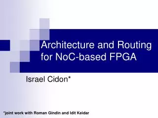
FPGA-based Prototyping of the Multi-Level Computing Architecture. presented by Davor Capalija Supervisor: Prof. Tarek S. Abdelrahman. Connections 2006. A modern processor. Superscalar, out-of-order and speculative execution. Control Unit. Instruction Queue. Memory. Register File. XU.

E N D
FPGA-based Prototyping of the Multi-Level Computing Architecture presented by Davor Capalija Supervisor: Prof. Tarek S. Abdelrahman Connections 2006
A modern processor • Superscalar, out-of-order and speculative execution Control Unit Instruction Queue Memory Register File XU XU XU Execution units
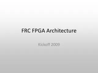
Multi-level Computing Architecture Control Program while(…) { Allocate(out frame) Preprocess(…) Analyze(…) Output(…) } Control Processor Task Scheduler Shared Memory Universal Register File PU PU PU Task instruction Analyze() Preprocess() Allocate() Tasks
Previous work in the MLCA group • Automatic task formation • Kirk Stewart • Compile-time optimizations to extract parallelism • Utku Aydonat • Task memory management • Ahmed Abdelkhalek • Power optimization using dynamic voltage scaling • Ivan Matosevic Work done using a high-level functional simulator
Motivation and goal • Realistic cycle-accurate evaluation using an FPGA-based prototype • Feasibility of hardware implementation • Deliver scalable performance • The control processor is expected to be a bottleneck • Custom hardware design of the control processor • Contribution: microarchitecture of the control processor
Challenges • Mapping the architecture to FPGA device resources • High requirements for on-chip memory: blocks, capacity & ports • System: shared memory, URF • PUs: caches, private and instruction memories • CP: renaming tables, task queues • Control processor microarchitecture design space • Performance vs. area trade-offs • Support for speculative execution of tasks
Status • Initial FGPA-based prototype • Nios II Development Board, Stratix Pro Edition (1S40) • Based on initial implementation by David Han • PUs - Altera Nios II/f processors • Interconnect - Altera Avalon interconnect • Memory - both on-chip & off-chip • Software-based control processor • Emulated on one Nios II/f processor • Determining and removing bottlenecks • Next step: microarchitecture of the Control Processor
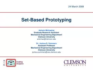
Bonus FPGA device Shared memory Universal Register File CP’s mem Ins4 M Priv4 M Ins1 M Priv1 M Ins3 M Priv3 M Ins2 M Priv2 M I$ D$ I$ D$ I$ D$ I$ D$ I$ D$ PU4 PU3 PU1 PU2 CP Comm4 Comm1 Comm2 Comm3 CP RT TQ