Download

1 / 12
120 likes | 220 Views
IBL @ October RRB. Slides for Marzio’s RRB talk CERN, October, 11 th 2010 G. Darbo & H. Pernegger. IBL Detector. Material from Raphael/Neal.

E N D
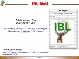
IBL @ October RRB Slides for Marzio’s RRB talk CERN, October, 11th 2010 G. Darbo & H. Pernegger
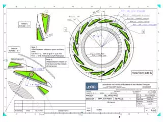
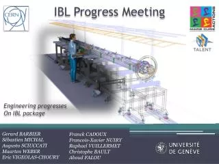
IBL Detector • Material from Raphael/Neal • The Insertable B-Layer (IBL) is a fourth layer added to the present Pixel detector between a new beam pipe and the current inner Pixel layer (B-layer). PP1 Collar Sealing service ring Alignment wires IBL key Specs/ Params • 14 staves, <R> = 33.25 mm • CO2 cooling, T < -15ºC @ 0.2 W/cm2 • X/X0 < 1.5 % (B-layer is 2.7 %) • 50 µmx 250 µm pixels • 1.8º overlap in ϕ, <2% gaps in Z • 32/16 single/double FE-I4 modules per stave • Radiation tolerance 5x10¹⁵ neq/cm2 IST IBL Support Tube IBL Staves
IBL Layout • Beam-pipe reduction: • Inner R: 29 25 mm • Very tight clearance: • “Hermetic” to straight tracks in Φ (1.8º overlap) • No overlap in Z: minimize gap between sensor active area. • Material budget: • IBL Layer (with IST): 1.5 % of X0 • Other Pixel layers: ~2.7 % of X0 • Beam-pipe (BP) extracted by cutting the flange on one side and sliding (guiding tube inside). • IBL Support Tube (IST) inserted. • IBL with smaller BP inserted in the IST
IBL Technical Design Report • ATLAS TDR includes: • Overview and motivation for the project • Study of the physics performance • Technical description of the project with baseline and options for critical issues • Three sensor technologies. • Beam-pipe, extraction/insertion, installation, ALARA. • Organization of the project and resources • Editorial team: M. Capeans (technical editor), G. Darbo, K. Einsweiller, M. Elsing, T. Flick,M. Garcia-Sciveres, C. Gemme,H. Pernegger, O. Rohne and R. Vuillermet. • Approved by the ATLAS Collaboration Board (October 2010 ATLAS Week) • 43 Institutions and 300 people in IBL CERN-LHCC-2010-13, ATLAS TDR 19
Physics Performance b-tagging with pile-up 2 jets of 500 GeV event with 2 x 1034 pile-up • b-tagging performance crucial for: • New Physics (3rd generation !) • observation of H → bb through boosted WH production • Main conclusions of IBL performance Task Force: • performance at 2x1034 with IBL is equal to or better than present ATLAS without pile-up • w/o IBL and 10% B-layer inefficiency: b-tagging ~ 3 times worse at 2x1034 than today Same event w/o pile-up IBL Physics & Performance Task Force – M. Elsing et al. IBL b-tagging with pile-up&inefficiencies
The New Front-end Chip (FE-I4) 60 KGD / Wafer 20.2 mm • Reason for a new front-end chip • Increased radiation hard (> 250 Mrad) • New architecture to reduce inefficiencies (L=2x1034): faster shaping; not move hits from pixel until LVL1 trigger. • Smaller pixel size 50 x 250 µm2 (achieved by 0.13 µm CMOS with 8 metals) • Larger fraction of footprint devoted to pixel array (~90%) – little space for IBL envelope. • FE-I4 submitted on July 1st • More than 2 years of engineering work for a team of >15 Engineers/physicist • Largest HEP chip ever! 20.2x19.0 mm2, 87 million transistors! • 60 Known Good Dies (KGD) / 8” wafer. • 16 wafer engineering run – 3 received and under test. • Money contributions collected following interim-MoU share. • Engineering run cost > 500kCH 160 336 rows FE-I3 (Pixel) FE-I4 (IBL) 18 19 mm 80 columns
Sensor Technologies for IBL • Three candidate sensor technologies address the IBL requirements with different trade-offs: • Prototyping with FE-I4 – qualification with irradiation (5x10¹⁵neq/cm2) and test beam – production yield Planar sensors (3 producers) • slim edge n-in-n & n-in-p • require the lowest temperature and high bias voltage. • have very well understood manufacturing sources, mechanical properties, relatively low cost, and high yield. • 3D sensors (3 producers) • Active edge, single/double side • require the lowest bias voltage, intermediate operating temperature, and achieve the highest acceptance due to active edges. • their manufacturability with high yield and good uniformity must be demonstrated. • Diamond sensors (2 producers) • polycrystalline CVD (pCVD) • require the least cooling and have similar bias voltage requirements to planar sensors. • their manufacturability with high yield, moderate cost, and good uniformity must all be demonstrated. Selection in summer 2011 450 µm n-in-n slim edge IBL layout Planar Sensor IBL FE-I4 diamond sensors Thin n-in-p 3D column 11 µm 3D Sensor ATLAS Pixel FE-I3 diamond module
History of IBL Project - Time Line • 1998: Pixel TDR • B-layer designed to be substituted every 3 years of nominal LHC (300 fb-1): due to then available radiation hard sensor and electronic technologies. • 2002: B-layer replacement • became part of ATLAS planning and was put into the M&O budget to RRB. • 2008: B-layer taskforce • B-layer replacement cannot be done – Engineering changes to fulfil delayed on-detector electronics (FE-I3, MCC) made it impossible even in a long shut down. • Best (only viable) solution: “make a new smaller radius B-layer insertion using technology being developed for HL-LHC prototypes”. This became the IBL. • 2009: ATLAS started IBL project: • February: endorsed IBL PL and TC • April: IBL organization in place (Endorsed by the ATLAS EB) • 2010: TDR and interim-MoU • TDR is under approval in ATLAS • Interim-MoU is collecting last signatures.
Interim-MoU - Institutions • There are 43 institutions in the IBL project • Large interest for the sensor (22 Institutions) • Full effort and funding requirements are covered • 300 people have expressed their interest to contribute to the project • many have already started to work. • In most cases institutes contribute with money where also there is contribution with manpower.
Management Board (MB) • MB ad-interim membership • IBL Project Leader: G. Darbo • IBL Technical Coordinator: H. Pernegger • “Module” WG (2 Physicists): F. Hügging & M. Garcia-Sciveres • “Stave” WG (1 Phy. + 1 M.E.): O. Rohne + D. Giugni • “IBL Assembly & Installation” WG (2 M.E. initially, a Phy. Later): F. Cadoux + R. Vuillermet • “Off-detector” WG (1 Phy. + 1 E.E.): T. Flick + S. Débieux • “Extra” members: • IBL/Pixel “liaison”: Off-line SW: A. Andreazza, DAQ: P. Morettini, DCS: S. Kersten • Ex officio: Upgrade Coordinator (N. Hessey), PO Chair (M. Nessi), Pixel PL (B. Di Girolamo), ID PL (P. Wells), IB Chair (C. Gößling) • IBL Management Board (MB) • Membership: • IBL PL + IBL TC • 2 cordinators from each WG • Plus “extra” members • Module WG • (2 cordinators) • FE-I4 • Sensors • Bump-Bonding • Modules • Procurement & QC • Irradiation & Test Beam • Stave WG • (1 Phys + 1 Eng.) • Staves • Cooling Design & Stave TM • HDI (Flex Hybrid) • Internal services • Loaded stave • Procurement & QC • Integration & Installation WG • (2 Eng.) • Stave Integration • Global Supports • BP procurement • Ext. services inst. • BP extraction • IBL+BP Installation • Cooling Plant • Off-detector • (1 Phys + 1 E.Eng.) • BOC/ROD • Power chain & PP2 • DCS & interlocks • Opto-link • Ext. serv .design/proc. • Procurement & QC • System Test