Download
1 / 20
200 likes | 220 Views
IBL Technical Aspects. H. Pernegger / CERN. Introduction. IBL detector is physically small (0.2m 2 active area) but requires several new technologies The specifications for the IBL are driven by expected radiation fluence, hit rate, proximity to beam axis and tight space constraints

E N D
IBL Technical Aspects H. Pernegger / CERN
Introduction • IBL detector is physically small (0.2m2 active area) but requires several new technologies • The specifications for the IBL are driven by expected radiation fluence, hit rate, proximity to beam axis and tight space constraints • The IBL is also a technology step to HL-LHC • Radiation hardness (incl. safety factor x2) ~ 5 x 10¹⁵ neq/cm2 • Frontend IC4: go to IBM 130nm process and improve readout architecture to minimize inefficiency at high hit rates and radiation hardness • Radiation hard Sensors: 3D silicon sensors, new planar sensors and CVD diamond sensors as possible options for radhard detectors • Readout system: improve data through-put and redundancy. • Cooling system & Mechanics: more efficient cooling of sensors+chips and significant reduction in X0 on staves.
IBL Modules Common sensor baseline for engineering and system purposes 3D sensors Single chip modules Planar/Diamond sensors Two chip module Module engineering parameters Sensor bias maximum 1000V Power dissipation in Sensor < 200mW/cm2 normalized at -15C Sensor temperature ~ -15C after full irradiation Sensors/Module prototype for ~10% of the detector in 2010/11 Single chip module: Edge < 325 um Double chip module: Edge < 450 um
IBL Sensor Prototyping Will produce qualification modules with planar, 3D, diamond sensors this year as soon as we get FEI4’s to test chip and sensors to IBL specs Main sensors in production for all three technologies: Planar • N-in-N conservative edge and N-in-N slim edge (CiS) Delivery Sept 25 • Thin n-in-p (HLL, HPK) Delivery End Sept • 60 single-chip & 30 double chip modules envisaged 3D • Active edge sensors preferred and in production by Sintef/SLAC, CNM, FBK • Double sided 3D also in production as backup • Sensor deliveries from End Oct 2010 to Spring 2011 • 60 single-chip modules envisaged Diamond • Polycrystalline CVD diamond sensors available from DDL and II-VI (total ~ 20) • 6 Delivered and at IZM for UBM, more available • 20 single-chip modules envisaged
FE-I4 readout chip (IBM 130nm) • Reason for a new FE design: • Increased rad hard • New architecture to reduce inefficiencies (L=2x1034) • Biggest chip in HEP to date • Greater fraction of footprint devoted to pixel array (~90%) • Lower power/pixel: don’t move the hits around unless triggered • Able to take higher hit rate: store the hits locally in each pixel and distribute the trigger • Submitted July 2010; Delivery confirmed for Sept. 23 • Final FE-I4B production chip ~ 1 year from now
FE-I4 Testing and bump-bonding of prototype modules • 1/2 wafer diced for test on single chip test cards (without sensors) • First wafers to IZM for first batch of prototype modules during October and to single-chip test cards for FE-I4 tests • USB based test system for FEI4 chip, module and wafer tests in place • Bump bonding with first 8 FEI4 wafers • Step 1: demonstrate that FEI4 works with sensors (lab measurements, irradiation, testbeam) (conservative chip thickness) • Step 2: Advanced module prototypes with thin chips, multi-chip modules, removal of handling wafers Want to minimize chip thickness to save material: <200mm , target: 100mm IZM devised special handling-wafer technique to allow solder BB of large but thin chips First successful results with 90mm thick chips in ~FE-I4 size chip
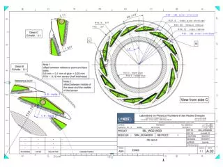
IBL Stave and Cooling 3mm CF pipe stave light foam • Stave construction • CF Shell (“Omega”) 300mm for stiffness • Ti pipe (ID 2mm wall 100mm): light and high thermal conductivity • Carbon foam as filler for module cooling • Thermo-mechanical tests with prototype staves with CF and Ti pipes nearly completed • Pipe + heaters -> measure HTC • Stave + heater -> measure thermal conductivity of assembly • CO2 cooling of staves with Ti pipes for IBL • Based on LHCb design, total power in IBL ~1.5kW • Smaller diameter cooling pipe and lighter coolant to reduce mass • Lower coolant temperature (-40C) • All inside connections welded (Ti-Ti joint TIG and EB) • Each stave = 1 cooling loop 2mm Ti pipe stave light foam
IBL material budget Radiation length: • Module and stave with chip target thickness: 1.16% • IST: CF tube center (0.5mm) : 0.28 % (not incl. shielding foil) Total currently: 1.44 % using 250 (sensor) +90 (chip) mm silicon
Stave Flex: power and readout modules Proceed with two designs in parallel at the moment: • Multilayer design. • Thin Kapton/Al. • Prototypes exist - main focus is test and simulation of electrical performance Loading of Modules • Carry out trial loadings to optimize glue dispersion and module placement • Flex connects to module through wrap-around “wing” • Wire-bonded after loading to module flex. CMD+CLK HV NTC Low voltages HV Ret Data Out
Stave support and integration with Beam pipe Integrate staves and services around beam pipe on surface (ATLAS SR1) 4-point support of IBL inside IST similar to present pixel detector
Beam pipe IP Pixel Package VI VA VT • Center (VI) beam pipe with “split flange” • 25 mm IR • Reduced flange diameter to fit with present pixel detector and IST • VA section planned to be changed in 2012 shutdown • Extraction of present beam pipe with long guiding tube
Beam pipe removal and Installation Problem: BP sags much more than clearance to B-layer once wires are removed Use pre-tensioned Brandeis Long Guide Tube – minimize sagging of BP Exercise and qualify all steps on existing mockup in Bat 180 6 meters Al (!) prototype 55 OD 50 ID with tension rod inside has been built No tension: |y| ~15mm With tension: |y| ~ 2mm
Off-detector: readout VME readout cards are under development ROD card having a Virtex5 controllerand Spartan6 data handling chips BOC card having a Virtex5 for all functions Firmware work in progress: developed and define consistent ROD+BOC FW concept PPC in FPGA modeling started ROD FPGA code : explore function and size of code Adoption of existing firmware to IBL usage started BOC detector interface firmware under development (TX and RX) Hardware developments Design of ROD first prototype board has started BOC test board for interfaces is ready S-Link Virtex5 Timing, Control, En-, Decoding, … Data from/to ROD TX RX ELMB CAN Bus
Milestones Detailed Schedule available at sharepoint: https://espace.cern.ch/atlas-ibl/Shared%20Documents/IBL-Schedule-DraftV3-4-14-06-2010.pdf Main dates • FEI4 submission : July 2010 • sensor choice June 2011 • FEI4 Version 2 eng. submission Sep 2011 • first prod module Nov 2012 • last prod module Sep 2013 • Stave loading completed (incl. contingency) June 2014 • IBL installation on or after May 2015
Schedule: Staves, Integration, Installation Service installation (USA15 to detector) Plan to install services up to detector during opening in 2012 shutdown Two contingency periods included in schedule Stave completion: 3 months in 2014 End of surface integration: 3 months in 2015
Summary FE-I4 design completed and submitted to IBM. Will receive chips this week – this is a major milestone for IBL project Sensors three sensor technology IBL prototype sensors are in production (planar, 3D, diamond). We will decide sensor technology summer 2011 based on test results with prototype modules and sensor+module production experience Prototype module plan to build significant number (>100) of modules to test bump bonding of thin modules , module performance, module on staves loading and operation of staves Stave we have constructed >10 prototype staves (CF pipes, Ti pipes) and tested thermal performance -> will use staves with Ti pipes and CO2 cooling Material budget: X/X0 = 1.16% of loaded staves, X/X0 ~ 1.5 of IBL with full support Integration and Installation Will integrate IBL around new beam pipe (IR 25mm) on surface Installation of IBL + all beam pipe operations to be exercised on mockup in Bat 18 Installation planned for 2016 shutdown Scheduled completion mid 2015 including contingency
Sensor technologies for IBL • Present ATLAS n-in-n sensors were designed to ~1x10¹⁵neq/cm2 and we have good production and operation experience with them • Their design was modified to become suitable for IBL specs • Reduction of dead edges to maximize sensitive area • Operation at higher voltages • New sensor technologies, which are being developed for HL-LHC, promise significant advantages: Thin n-in-p, 3D silicon, CVD diamonds • Active edges or slim edges • Lower depletion voltages • Less cooling requirements • The IBL can benefit from those advantages if we can show that • The sensors work well with the FEI4 chip up to highest fluences • The modules can be operated reliably • The manufacturing of high quality sensors and modules with reasonable yield is possible • We therefore decided to prototype a significant number modules with different technologies until the sensor technology needs to be decided for pre-production (~June 2011)
Sensor technologies for IBL Diamonds Planar silicon 3D silicon Active edge single sided and double sided Prototyping with CNM, Sintef/SLAC, FBK • Polycrystalline CVD diamonds • Prototyping with DDL and II-VI • Slim edge n-in-n • Thin n-in-p • Prototyping with CiS, HLL, HPK 450um N-in-n slim edge Growth side Substrate side Thin n-in-p ATLAS Pixel FE-I3 diamond module 100um