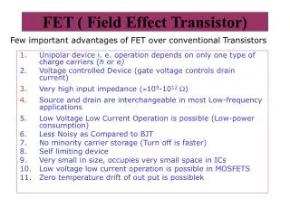
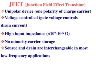
Download
1 / 41
420 likes | 450 Views
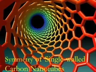
Field Effect Transistor Behaviour in Single Wall Carbon Nanotubes and Peapods. Isaac Newton Institute Workshop, Cambridge 27-30 September 2004. Poul Erik Lindelof Niels Bohr Institute, Nano-Science Center, University of Copenhagen.

E N D
Field Effect Transistor Behaviour in Single Wall Carbon Nanotubes and Peapods Isaac Newton Institute Workshop, Cambridge 27-30 September 2004 Poul Erik Lindelof Niels Bohr Institute, Nano-Science Center, University of Copenhagen Niels Bohr Institute
Field Effect Transistor Behaviour in Single Wall Carbon Nanotubes and PeapodsPoul Erik LindelofNiels Bohr Institute, Nano-Science Center, University of Copenhagen Henrik Ingerslev Jørgensen, PhD student Jonas Rahlf Hauptmann, PhD-student Thomas Sand Jespersen, PhD-student Kasper Grove-Rasmussen, Ph.D.-student (p.t. visiting NTT BRL, Japan) Ane Jensen, Dr Jesper Nygård, Dr & collaboration with Andrei Khlobystov, Oxford University Niels Bohr Institute
Field Effect Transistor Behaviour in Single Wall Carbon Nanotubes and Peapods Outline of talk: Importance of contacts, Coulomb blockade, odd-even effects due to spin Zeeman splitting, ESR? Kondo effect Hybrids with GaAs Magnetic contacts Peapods, Periodic modulation Summary Niels Bohr Institute
3 carbon nanotubes (10,10) (15,0) (12,8) Niels Bohr Institute
TEM of carbon nanotube robe A nanotube (or two?) TEM picture 20 nm Niels Bohr Institute
Assignment by Raman spectra Thomas Sand Jespersen, MSc thesis Niels Bohr Institute
although carbon atoms only! Contact configuration 2-point Electrical Resistance drain • Au/Ti contacts • Carbon nanotube • Silicondioxide (300 nm) • Highly doped silicon source gate Niels Bohr Institute
Contacting a SWCNT 10µm 50µm Niels Bohr Institute
SWCNT, metals or semiconductors Niels Bohr Institute
3 examples of Contact resistances G300K = 0.3 e2/h G300K = 1.8 e2/h G300K = 3 e2/h T = 1K Theoretical maximum Gmax = 4 e2/h T = 100mK Niels Bohr Institute
Metallic SWCNT, Temperature Dependence P.E. Lindelof, et al., Physica Scripta T02, 22 (2002) Niels Bohr Institute
Odd-Even Additional energies D.H. Cobden and J. Nygård Phys,Rev,Lett. 89, 046803 (2002) Niels Bohr Institute
Bias Spectroscopy, Zeeman splitting 0T a b 6T P.E. Lindelof , et al., Physica Scripta T02, 22 (2002) Niels Bohr Institute
Wolfgang Pauli and Niels Bohr 1951, looking at a spinning object! Niels Bohr Institute
E O E O E O E Q eV D P Q P Kondo bias spectroscopy J. Nygård et al., Nature 408,342 (2000) Niels Bohr Institute
c a b G0 (e2/h) TK (K) a 1.72 1.6 b1.77 0.9 Kondo temperature J. Nygård et al., Nature 408, 342 (2000) Niels Bohr Institute
Carbon nanotube inside a MBE GaAlAs single crystall = + A. Jensen, J.Hauptmann, J, Nygård, J. Sadowski, P.E. Lindelof, Nano Letters (2004) Niels Bohr Institute
MBE chamber Device fabrication MBE grown substrate: - n-doped GaAs - insulating superlattice barrier - amorphous As cap (protection) Dispersion of single-wall nanotubes from suspension, ambient conditions Niels Bohr Institute
MBE chamber Device fabrication Epitaxal overgrowth with Ga0.95Mn0.05As by MBE at 250 C Result: nanotubes incorporated in GaAs sandwich Reloaded in the MBE chamber Desorption of As cap at 400 C, leaving the nanotubes on the clean GaAs crystal surface Niels Bohr Institute
Mesa, Trench etch, SWCNTs Trench and SWCNT Niels Bohr Institute
Device architecture Au/Zn a) b) (Ga,Mn)As 7 SWNT 5 4 6 Cr/Au 3 x100 2 AlAs 1 GaAs Niels Bohr Institute
Configurations in various magnetic fields Niels Bohr Institute
GaAs GaAs AFM scan of SWCNT between MBE grown GaAs electrodes Single wall carbon nanotube The trench is 0.5 µm wide Niels Bohr Institute
G(Vg,B) for GaMnAs-SWCNT-GaMnAs Niels Bohr Institute
G(Vsd,B,T) for GaMnAs-SWCNT-GaMnAs Niels Bohr Institute
Magnetoresistance of GaMnAs-SWCNT-Au Niels Bohr Institute
Juliere’s model n(1,+) n(1,-) n(2,+) n(2,-) G(++)~n(1,+)n(2,+)+n(1,-)n(2,-) G(+ -)~n(1,+)n(2,-)+n(1,-)n(2,+) P(1)=[n(1,+)-n(1,-)]/[n(1,+)+n(1,-)] DG/G=[G(++)-G(+ -)]/G(++) =2P(1)P(2)/[1+P(1)P(2)] >0 Negative magnetoresistance Niels Bohr Institute
Tunnelling into two domains (Streda, unpublished) T(1,-) Tt T(1,+) T(2,-)= T(2,-) T(1,+)=pT1, T(1,-)=(1-p)T1, T(2,+)=T(2,-)=T2 G(p=1)=G(+)+G(-)=T1TtT2/[Tt(T1+T2)+2T1T2] G(p=1)-G(p=½)= -G(p=1)[T1/T2 + 2T1/Tt] magnetoresistance>0 Niels Bohr Institute
C-60@SWCNT Peapod K. Haldrup, A.N. Khlobystov et al. Niels Bohr Institute
Raman spectra a) SWCNT b) SWCNT - through treatment c) C-60@SWCNT Peapod - through treatment Niels Bohr Institute
Peapod Conductance vs. Vg Niels Bohr Institute
G(290) vs. power law exponent.C-60@SWCNT (O) & SWCNT (l) Haldrup, Khlobystov et al., To be published Niels Bohr Institute
Nanometer periodic modulation of potential along SWCNT Thomas Sand Jespersen, Poul Erik Lindelof, unpublished Niels Bohr Institute
MBE growth of SL with guiding structures. Cleaved Edge Overgrowth Niels Bohr Institute
AFM picture of cleaved and etched surface Niels Bohr Institute
AFM study of 30 nm period superlattice on the cleaved edge Niels Bohr Institute
Carbon nanotube decoration of CEO SL surface Niels Bohr Institute
SWCNT superlattice Raman spectrum.No data for the combination yet. Niels Bohr Institute
Summary The contact resistance to metallic carbon nanotubes, Temperature dependence of electrical conductance Odd-even Coulomb blockade conductance peaks Zeeman splitting (g=2) Spin ½ co-tunneling (Kondo effect) GaAs-CNT hybrids, magnetic contacts Peapods, CEO periodic modulation Niels Bohr Institute
Movie of ”spinning object” Niels Bohr Institute
The ”spinning object” in action Niels Bohr Institute