Download
1 / 32
320 likes | 441 Views
Michal Szelezniak 1 on behalf of: E. Anderssen 1 , X. Dong 1 , L. Greiner 1 , J. Kapitan 2 ,S. Margetis 3 , H. Matis 1 , H.G. Ritter 1 , J. Silber 1 , T. Stezelberger 1 , X. Sun 1 , F. Videbaek 4 , Ch. Vu 1 , H. Wieman 1 , Y. Zhang 1 1 LBNL, 2 NPI ASCR, 3 KSU, 4 BNL.

E N D
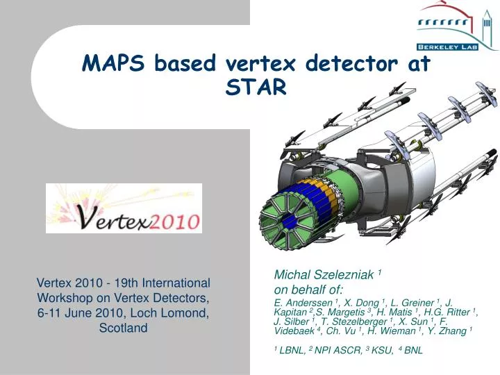
Michal Szelezniak 1 on behalf of: E. Anderssen 1, X. Dong 1, L. Greiner 1, J. Kapitan 2,S. Margetis 3, H. Matis 1, H.G. Ritter 1, J. Silber 1, T. Stezelberger 1, X. Sun 1, F. Videbaek 4, Ch. Vu 1, H. Wieman 1, Y. Zhang 1 1 LBNL, 2 NPI ASCR, 3 KSU, 4 BNL MAPS based vertex detector at STAR Vertex 2010 - 19th International Workshop on Vertex Detectors, 6-11 June 2010, Loch Lomond, Scotland
Outline • STAR HFT Upgrade • PIXEL (PXL) Requirements • PIXEL Geometry • PIXEL Development Path • Sensors • RDO electronics • Mechanical support – cooling tests • Readout cable development • Summary and Outlook
STAR Heavy Flavor Tracker (HFT) Upgrade The HFT is a tracking upgrade to the STAR detector to identify mid rapidity Charm and Beauty mesons and baryons through direct reconstruction and measurement of the displaced vertex with excellent pointing resolution. TPC – Time Projection Chamber (main detector in STAR) HFT – Heavy Flavor Tracker • SSD – Silicon Strip Detector • IST – Inner Silicon Tracker • PXL – Pixel Detector (PIXEL) Graded resolution: TPC→SSD → IST → PXL ~1mm ↘ ~300µm ↘ ~250µm ↘ <30µm
PIXEL Requirements critical and difficult
PIXEL Geometry The detector ladders are 50 µm thinned silicon, on a flex kapton/aluminum cable. 8 cm radius End view 20 cm 2.5 cm radius Inner layer Outer layer Cantilevered support coverage ±1 One of two half cylinders Total: 40 ladders
PIXEL Prototype Development Path Small scale prototypes Full – reticle prototypes Pre-production prototype Sensor development ADC based readout Binary readout of all pixels Digital RDO + zero suppression Ladder readout Readout development Probe tests Probe tests Ladder prototype Cable development Cooling & vibration tests Mechanical development Sector prototype Prototype detector
PIXEL Prototype Development Path Small scale prototypes Full – reticle prototypes Pre-production prototype Sensor development ADC based readout Binary readout of all pixels Digital RDO + zero suppression Ladder readout Readout development Probe tests Probe tests Ladder prototype Cable development Cooling & vibration tests Mechanical development Sector prototype Prototype detector
MAPS Prototypes For PIXEL Designed by IPHC PIXEL benefits from the continuous MAPS development at IPHC. • Next generation (in design) • Current generation • Phase-1 prototype • Reticle size (~ 4 cm²) • Pixel pitch 30 μm • ~ 410 k pixels • Column parallel readout • Column discriminators • Binary readout of all pixels • Data multiplexed onto 4 LVDS outputs @ 160 MHz • Integration time 640 μs • Functionality tests and yield look very good. • Measured ENC is 15 e-. • Beam test to measure MIP efficiency planned for 2010. • Phase-2 prototype • Small mask adjustments to improve discriminator threshold dispersion • Design based on Mimosa26 architecture • Reticle size (~ 4 cm²) • Pixel pitch 20.7 μm (recent change) • 890 k pixels • Reduced power dissipation • Vdd: 3.0 V • Optimized pixel pitch vs. Non-ionising radiation tolerance • Estimated power consumption ~134 mW/cm² • Short integration time 185.6 μs • Improved pixel architecture • Optimized discriminator timing • Improved threshold uniformity • on-chip zero suppression • 2 LVDS data outputs @ 160 MHz
Probe Tests • Sensors designed with dedicated probe pads in the sensor pad ring. • Automated test system allows for a qualitative analysis of probed sensors. • Including identification of dead/stuck pixels • 13 full-thickness, diced sensors probe tested. • Results are very promising. • Up to 3 probe tests on a sensor. • We will begin testing thinned sensors within the next few days Testing diced and thinned sensors to meet yield requirements for ladder assembly Vacuum chuck for probe testing 50 μm thick MAPS Phase-1 discriminator transfer functions ƒ(threshold voltage) observed on two of the probed sensors : Initial testing with ~75 μm travel past touchdown 30 μm additional lowering of probe pins We are considering possibility of using pad protection diodes to verify good contacts
PIXEL RDO Basic Unit 6 m (24 AWG TP) 2 m (42 AWG TP) PIXEL RDO architecture validated with data path test Mass termination board + latch up protected power daughtercard ← Front Back ↓ 100 m (fiber optic) RDO PC with DDL link to RDO board RDO motherboard + Xilinx Virtex-5 Dev Board • 4 ladders per sector • 1 Mass Termination Board (MTB) per sector • 1 sector per RDO board • 10 RDO boards in the PIXEL system Measured BER (bit error rate) of < 10-14
PIXEL Mechanical Support other requirements: • Fast detector replacement capabilities • Air cooling Mechanical stability within a 20 μm window is required. • A well controlled method for installation of the pixel detector has been developed with emphasis on ease of operation and avoidance of detector risk • Insertion mechanism to guide detector around beam pipe and beam pipe support uses track and carriage with hinge and cam to guide into final docking position defined by locking kinematic mounts
PIXEL Thermal Analysis and Testing The large CTE difference between silicon and kapton is a potential source of thermal induced deformation. An air-flow based cooling system has been chosen for PIXEL to minimize material budget. low mass region • Silicon power: 100 raised to 170 mW/cm2 (~ power of sunlight) • 350 W total in the low mass region (Si + drivers) Detector mockup to study cooling efficiency CFD computational fluid dynamics
Detector Mockup Driver section ~ 6 cm Sensor section ~20 cm • Kapton cables with copper traces forming heaters allow us to dissipate the expected amount of power in the detector • 6 thermistors on each ladder • One of the sectors (sector 1) was equipped with 10 dummy silicon chips per ladder, with Pt heaters deposited on top of silicon Thermal camera image of sector 1: Power ~340 W Airflow 10.1 m/s
Cooling Tests at ~340 W unsuported end mid-section fixed end Solid – inner layer Open – outer layer • Measurement results agree with simulations • Air flow-induced vibrations (@ < 10 m/s) are within required stability window
Sensor RDO Cable Development Al based cable is needed for low radiation length in the low mass region. PIXEL Cable development stages: • Infrastructure testing board • Prototype detector cable FR-4 with Cu traces • Prototype detector cable Kapton with Cu traces • Prototype detector cable Kapton with Al traces Side view (exaggerated vertical scale) Preliminary Design: Hybrid Copper / Aluminum conductor flex cable Driver region Low mass Sensor region Low mass region calculated X/X0 for Al conductor = 0.073 % Low mass region calculated X/X0 for Cu conductor = 0.232 % • A detailed description of the challenge is available at http://rnc.lbl.gov/hft/hardware/docs/PXL_RDO_cable_options_1.doc
Infrastructure Test Board • This is a ladder level system test • complete chain of RDO system that has never been fully tested (MTB, RDO, long cables) • Multidrop clock working • JTAG daisy chain working (with caveats) • Just started taking data Ladder-like layout except for Power and GND Very preliminary results with full thickness Phase-1 prototypes: preliminary • Coupling mechanism is under investigation. • Next board with 50 μm Phase-2 prototypes is being assembled.
Summary and Outlook • Development of the detector’s mechanical support is well advanced • Very low mass detector support designs have passed multiple analysis tests and prototype tests addressing cooling and position stability. • Prototype tooling is in place and tested for sector/ladder production. • Concept designs for installation and insertion are well advanced . • MAPS technology development at IPHC is well advanced and on schedule • The RDO data path architecture has been validated and hardware prototypes have been produced • Testing of individual sensors works well. • We have just started reading out 10 sensor ladders. • Test plans: • Beam test with Phase-2 @ Fermilab • HFT is headed for CD2/3 in Q4 FY2010 • HFT completion scheduled for Q3 FY 2013
Vacuum chuck Vacuum chuck for probe testing 50 μm thick MAPS
Stability requirement drives design choices • The detector ladders are thinned silicon, on a flex kapton/aluminum cable • The large CTE difference between silicon and kapton is a potential source of thermal induced deformation even with modest 10-15 deg C temperature swings • Two methods of control • ALICE style carbon composite sector support beam with large moment of inertia • Soft decoupling adhesive bonding ladder layers
RDO requirements • Triggered detector system fitting into existing STAR infrastructure (Trigger, DAQ, etc.) • Deliver full frame events to STAR DAQ for event building at approximately the same rate as the TPC (1 kHz for DAQ1000). • Have live time characteristics such that the Pixel detector is live whenever the TPC is live. • Reduce the total data rate of the PXL detector to a manageable level (< TPC rate of ~1MB / event). • Contain additional functionality for full sensor characterization including production probe testing.
Monolithic Active Pixel Sensors MAPS pixel cross-section (not to scale) • Standard commercial CMOS technology • Room temperature operation • Sensor and signal processing are integrated in the same silicon wafer • Signal is created in the low-doped epitaxial layer (typically ~10-15 μm) → MIP signal is limited to <1000 electrons • Charge collection is mainly through thermal diffusion (~100 ns), reflective boundaries at p-well and substrate → cluster size is about ~10 pixels (20-30 μm pitch) • 100% fill-factor • Fast readout • Proven thinning to 50 micron
Vibrations caused by airflow coupled means that the unsupported end is tied to sector 2 • Sector 1, Ladder 2 (coupled ) (coupled ) (coupled ) Beginning of the driver section (Supported end) End of sensor section (Unsupported end)
3 µm 3 µm 2 µm 8 µm 4 µm 11 µm HFT PXL status – air flow vibration tests carbon fiber sector beam capacitance vibration probe two positions shown air in air out adjustable wall for air turn around reinforced end no reinforcement at the end air velocity probe two positions shown
LVDS Data Path Testing at 160 MHz 42 AWG wires Ladder mock-up with 1-to-4 LVDS fanout buffers Mass termination board + LU monitoring 24 AWG wires 2 ns eye pattern opening for 1 m 42 AWG cables at 200 MHz Virtex-5 based RDO system with DDL link to PC • Data Path Architecture Validated • Measured BER (bit error rate) of < 10-14
Sensor RDO Cable Development • A detailed description of the challenge is available here http://rnc.lbl.gov/hft/hardware/docs/PXL_RDO_cable_options_1.doc • A single sided test cable design has been produced for fabrication at Datex to assess capability and quality. • Some delay due to material issues. It is difficult to find anyone willing to fabricate kapton/Al. • We have located some 1 mil Al on 1 mil mylar and shipped it to Datex. They are evaluating the suitability. • Datex is about to start first attempt at fabrication. • Other vendors (SE SRTIIE, Kharkov,Ukraine and CERN?) will be contacted.
Project status Formal Department of Energy (DOE) milestones: • CD-0 (Critical Decision-0, Mission Need) approved in Feb 2009 • CD-1 review in Nov 2009. (“One of the alternatives proposed in the CD-0 is selected and a credible cost range is established”) • CD-1 homework sent to DOE, waiting for approval • Ready for CD 2/3 in Q4FY10 (Performance Baseline / Start of Construction) • Next step in DOE approval process. HFT will become a full construction project and construction funds will be released upon successful completion. • Requires a significant amount of technical and management documentation to be generated. • HFT completion scheduled for Q3 FY 2013