Download
1 / 34
340 likes | 515 Views
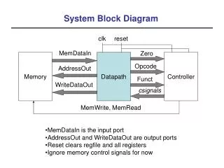
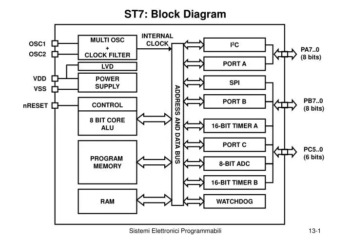
ST7: Block Diagram. INTERNAL CLOCK. MULTI OSC + CLOCK FILTER. I 2 C. OSC1. PA7..0 (8 bits). OSC2. PORT A. LVD. VDD. POWER SUPPLY. SPI. VSS. PORT B. PB7..0 (8 bits). CONTROL 8 BIT CORE ALU. nRESET. ADDRESS AND DATA BUS. 16-BIT TIMER A. PORT C. PROGRAM MEMORY. PC5..0

E N D
ST7: Block Diagram INTERNAL CLOCK MULTI OSC + CLOCK FILTER I2C OSC1 PA7..0 (8 bits) OSC2 PORT A LVD VDD POWER SUPPLY SPI VSS PORT B PB7..0 (8 bits) CONTROL 8 BIT CORE ALU nRESET ADDRESS AND DATA BUS 16-BIT TIMER A PORT C PROGRAM MEMORY PC5..0 (6 bits) 8-BIT ADC 16-BIT TIMER B RAM WATCHDOG Sistemi Elettronici Programmabili
ST72254 - Package Sistemi Elettronici Programmabili
ST72254 Memory Map Sistemi Elettronici Programmabili
ST72254 – Interrupt Vector Sistemi Elettronici Programmabili
ST72254 Registers (1) Sistemi Elettronici Programmabili
ST72254 Registers (2) Sistemi Elettronici Programmabili
ST72254 Registers (IO) Sistemi Elettronici Programmabili
ST72254 Registers (Timer) Sistemi Elettronici Programmabili
ST72254 Registers (ADC) Sistemi Elettronici Programmabili
IO Port: Block Diagram Sistemi Elettronici Programmabili
IO Port Configurations - Input Sistemi Elettronici Programmabili
IO Port Configurations – Output Opendrain Sistemi Elettronici Programmabili
IO Port Configurations – Output Push Pull Sistemi Elettronici Programmabili
IO Port: Registers Sistemi Elettronici Programmabili
8-BIT SUCCESSIVE APPROXIMATIONS CONVERTER WITH UP TO 8 ANALOG CHANNELS FEATURE : Accuracy : 1 LSB Total Unajusted Error MAX : 1 LSB Conversion time : 24 CPU cycle ie 3µs at full speed (8MHz) FLAGS COCO : end of conversion (Status flag) ADON : ADC on/off bit (to reduce power consumption) ADC: Overview (1) Sistemi Elettronici Programmabili
LOW CONSUMPTION MODES Wait mode doesn't affect the ADC Halt mode stops the ADC. HARDWARE ST72334 and ST725xx : Vdda and Vssa must be connected externally respectivelly to Vdd and Vss through decoupling capacitors. ST72254 : connection done internally RATIOMETRIC In the Functionnal Range If analog voltage input > Vdd :converted result = FFh (no overflow indication) If analog voltage input < Vss :converted result = 00h (no underflow indication) ADC: Overview (2) Sistemi Elettronici Programmabili
ADC: Block Diagram Sistemi Elettronici Programmabili
ADC: Registers Sistemi Elettronici Programmabili
Timer: Block Diagram Sistemi Elettronici Programmabili
Timer: Block Diagram (H) Sistemi Elettronici Programmabili
Timer: Block Diagram (L) Sistemi Elettronici Programmabili
Timer: Read Sequence Sistemi Elettronici Programmabili
Timer: Input Capture Sistemi Elettronici Programmabili
Timer: Output Compare Sistemi Elettronici Programmabili
Automatic generation of a Pulse Width Modulated signal Period &pulse lenght set by software: The first Output Compare Register OC1R contains the length of the pulse The second Output Compare Register OCR2 contains the period of the pulse Resolution up to 100 steps at 20 KHz (fCPU =4 MHz): 1% of accuracy on the duty cycle TIMER: PWM Mode t T Sistemi Elettronici Programmabili
Free running counter is initialized to FFFCh • OLVL2 bit level is applied on the OCMP1 pin • ICF1 bit is set When the free running counter reaches OC2R register value When the free running counter reaches OC1R register value • OLVL1 bit level is applied on the OCMP1 pin Timer: PWM Flow Sistemi Elettronici Programmabili
Timer: PWM Counter FREE RUNNING COUNTER VALUE Ttimer × 65535 Tmax = FFFFh FFFCh Compare 2 Compare 1 0000h time OLVL2= 1 OCMP1 Ouput Compare pin Timer output time OLVL1=0 Sistemi Elettronici Programmabili
Timer: CR1 Sistemi Elettronici Programmabili
Timer: CR2 Sistemi Elettronici Programmabili
Timer: SR Sistemi Elettronici Programmabili
Schmitt Trigger: Caratteristica Inverter Vin t Vout t Sistemi Elettronici Programmabili Sistemi Elettronici Programmabili 13-31
Schmitt Trigger: Caratteristica Vout Vin Sistemi Elettronici Programmabili
Schmitt Trigger: Inverter - Commutazioni Spurie Vin t Vout t Sistemi Elettronici Programmabili
Schmitt Trigger: Commutazione Vin t Vout t Sistemi Elettronici Programmabili