Download
1 / 41
440 likes | 502 Views
Memory and Programmable Logic Devices. Chapter 6. Definitions. RAM – Random Access Memory ROM – Read Only memory PLD – Programmable Logic device ROM PLA – Programmable Logic Array PAL - Programmable Array Logic FPGA – Field Programmable Gate Array. Block Diagram of Memory.

E N D
Memory and Programmable Logic Devices Chapter 6
Definitions • RAM – Random Access Memory • ROM – Read Only memory • PLD – Programmable Logic device • ROM • PLA – Programmable Logic Array • PAL - Programmable Array Logic • FPGA – Field Programmable Gate Array
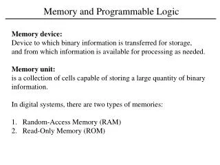
Block Diagram of Memory Number of bits in memory is referred as: K (kilo) - 210 M (mega) 220 G (giga) 230
Example 8388608 1048576 20 8 1024 10 4 4096 8388608 2097152 21 4 22 1 4194304 4194304 67108864 2097152 21 32 1048576 16384 14 64 8388608 23 8 67108864
Example 1024 X 16 memory 10 bits for addressing 16 bits for data
The steps for write are: Set the address lines Apply the data to the data input lines Activate the write input The steps for read are: Set the address lines Activate the read input Write and Read Operations
Timing Waveforms CPU rate is 50Mhz
Timing Waveforms Transfer data to a register
Properties of memory • Volatile • Information is lost when the power is turned off • RAM • Nonvolatile • Information is not lost when the power is turned off • Magnetic disks, ROM
Properties of memory RAM • Static RAM – SRAM • Consists of latches • faster • Dynamic RAM – DRAM • Consists of capacitors • Needs refreshing cycles • Reduced power consumption • Larger storage
Dynamic RAM IC • Because of its property of high storage at low cost DRAM dominates the high capacity applications. • Its working principal can be explained with an analogy.
Dynamic RAM IC • Reading is destructive • After reading previous value should be restored • To restore a value of 1, the large tank is filled and the valve is opened. • To restore a value of 0, big tank is emptied and the valve is opened to drain the storage tank.
Dynamic RAM IC • Even without read, due to leaks every storage cell must be refreshed before its level has declined to a point at which the stored value can no longer be properly observed. • Each row of DRAM requires refreshing within a maximum refresh time; typically ranging from 16 – 64 ms. • There are two modes of refreshing: • Distributed refreshing: refreshes are performed at evenly spaced points in the refresh time. • Burst refreshing: refreshes are performed one after the other.
Dynamic RAM IC - Example • Suppose we have 4Mx4 DRAM having refresh time of 64 ms, 4096 rows to refresh and the length of time for single refresh is 60 ns. • For distributed refresh 64ms/4096 = 15.6 microsec. • 60ns x 4096 = 0.25 ms is used for refreshing • For burst refreshing, refreshing time is 0.25 ms. For the same DRAM, the DRAM controller must initiate a refresh every 15.6 microseconds for distributed refresh and must initiate 4096 refreshes sequentially every 64 ms. for burst refresh. During any refresh cycle, no DRAM reads or writes can occur.
Dynamic RAM IC DRAM cell consists of a capacitor and one transistor. SRAM cell consists of 6 transistors. Thus DRAM has 3 times the capacity of SRAM And 1/3 less cost/bit.
Dynamic RAM IC DRM cell model DRM cell model Write Logic Read Logic
Building Memory Systems – Example 2 Build a 2Mx4 memory system using 1Mx4 memory chips. First identify the specifications for the 1Mx4 memory chips and the desired 2Mx4 memory system? As the table shows, the # of data lines are the same for both. • There is an extra address line in the 2Mx4 giving double the # of addresses and double the # of bits • Therefore, we require two 1Mx4 memory chips arranged where one address line is used to decode which 1Mx4 chip is enabled.
ROM • Four technologies are used for ROM programming • Mask programming – ROM • Fuses – programmable ROM, PROM • Erasable floating-gate technology- EPROM • Electrically erasable technology - EEPROM
Combinational Circuit Implementation • ROM includes a decoder and OR gates in itself • By closing connections for those minterms included in the function, the ROM outputs can be programmed to represent the Boolean functions of the output variables in a combinational circuit.
Combinational Circuit Implementation Example A7(I4, I3, I2, I1, I0) = m(0, 2, 3, …, 29) Closed connection includes the minterm, open connection excludes the minterm from the output function.
Combinational Circuit Implementation Design a combinational circuit that accepts a 3-bit number and generates its square on the outputs.
F1 = AB + AC + BC F2 = AB + AC + ABC Programmable Logic Array- Example F1(A, B, C) = m(0, 1, 2, 3, 4) F2(A, B, C) = m(0, 5, 6, 7)
PAL Devices The PAL device is a PLD with a fixed OR array and programmable AND array.
W = ABC + ABCD X = A + BCD Y = AB + CD + BD Z= ABC + ABCD + ACD + ABCD = W + ACD + ABCD PAL Devices- Example W(A, B, C, D) = m(2, 12,13) X(A, B, C, D) = m(7, 8, 9, 10, 11, 12, 13, 14, 15) Y(A, B, C, D) = m(0, 2, 3, 4, 5, 6, 7, 8, 10, 11, 15) Z(A, B, C, D) = m(1, 2, 8, 12, 13)