Download
1 / 7
80 likes | 93 Views
High Quality PCB Co., Limited is a leading of PCB(Printed Circuit Board) Manufacturer in China since 1995. Dedicate to the technologies innovation, being engaged in IC Substrates, High-Density Interconnect PCB, Multi-layer PCB, Rigid Flexible PCB, Flexible, Radiofrequency PCB. Both prototypes and mass production projects are available for High-Quality PCB.

E N D
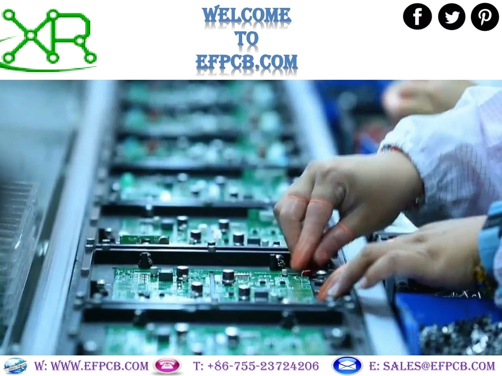
WELCOME TO efpcb.com W: www.efpcb.com T: +86-755-23724206 E: sales@efpcb.com
Using Computer Aided Design (CAD) software first the electronic diagram of the required circuit is prepared to make a custom PCB. After that using Computer Aided Manufacturing Software technology the gold finger PCB prototype is developed. FR4 High Temperature, FR4, GeTek, Polyimide, Arlon, Rogers, Alumina, Nelco, Bakelite, Ceramic, CEM5, CEM1, and FR1 are the common materials used for manufacturing PCBs. Upon the requirements of the circuit, the thickness and size of the board depend.
To assemble leaded electronic and electrical components holes are drilled into the board once the board is ready with copper traces. special tungsten carbide laser or drill bits are used for drilling. With hollow rivets, the holes made are filled or using an electroplating process are coated through and thus among the various layers, it forms an electrical connection.
Coating of the entire board with masking material, except pads and holes is the next step. Nickel, lead-free solder, lead solder, hard/deep gold, OSP, wire bondable gold, immersion gold, flash gold, immersion silver, carbon ink, immersion tin and SN 100CL, an alloy of tin, copper are the Materials commonly used for this purpose. Screen-printing is the last step, where on the plating gold PCB the text and legend are printed.
The most common type of board is this, where to both sides of the substrate components and parts are attached. Double-sided PCBs having connecting traces on both the sides are used in such cases. For assembly of components, through-hole construction is used for Double-sided Printed Circuit Boards or high volume PCB usually.
High Quality PCB Co., Limited Office address: ShajingTown,BaoanDistrict ,Shenzhen ,518000, China Plant 1 address: Building 5-6, Fu Qiao 3rd Industrial Zone, Bao' an, Shenzhen, Guangdong, China. Plant 2 address: Zhuhai, Guangdong,China Plant 3 address: Dongguan, Guangdong, China TEL: +86-755-23724206 Skype: shawnwang2006 Email: sales@efpcb.com http://efpcb.com/