Download
1 / 17
170 likes | 321 Views
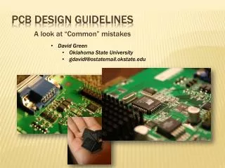
David Green Oklahoma State University gdavidl@ostatemail.okstate.edu. A look at “Common” mistakes. PCB guidelines. Interference to other devices may cause reliability issues, safety/health concerns, etc.

E N D
David Green • Oklahoma State University • gdavidl@ostatemail.okstate.edu A look at “Common” mistakes PCB guidelines
Interference to other devices may cause reliability issues, safety/health concerns, etc. Local interference on a PCB could cause increased bit error rate (BER), signal integrity problems, unintentional device resets/outages, voltage spikes, increased noise in on-board peripherals, etc. Is this important? Ever hear interference generated by your cellphone?
Return current is the #1 cause for EMI Remember, current flows in loops. can generate large high frequency harmonics What path does current take on the reference plane? For low frequencies return current follows a path of least resistance. For high frequencies current follows a path of least impedance. The impedance for an inductor increases with increasing frequency. Must take into consideration at high frequencies. “Ground is a place where potatoes and carrots thrive!” – Dr. Bruce Archambeault Overview of basic principles
Three critical functions: • Provides a stable voltage reference for digital signals • Distribute power to devices • Used to reduce interference between signal lines • As mentioned, low frequency return current follows path of least resistance, whereas high frequency current follows path of least impedance. • The overall goal is to reduce return current loop area. The Reference Plane • Some layout considerations: • Split plane – disrupts return current flow to excitation source. This can result in drastically increased emissions. • Placing holes in board for connector pins – Holes too big can essentially cause a split. This can be corrected by allowing space in between neighboring holes to allow return current to run through. • When running signal traces on the reference plane keep in mind their placement. Coupling can be reduced by placing signal lines perpendicular to traces on top of PCB.
Return Current Path Simulation frequency of 20 MHz… Sound familiar? Top of PCB Bottom of PCB
Measurements were performed in a fully anechoic chamber Split Reference Plane Measurements • Log periodic antenna used for far field measurements from 290 MHz – 2 GHz. • Dual Ridge Horn antenna used for 700 MHz to 4 GHz.
Reference plane Split Split Plane – DRG Split Plane – Log Periodic Solid Plane – DRG Solid Plane – Log Periodic
Simulation Vs. Measured Results Interesting! • So why the difference? • Source power of simulation is 13dBm, measured results are 18dBm • How do we really model connections, components, structures, etc? • Can we trust measurements?
Adding a stitching capacitor to plane Offset stitching capacitor Centered stitching capacitor • Obvious difference between placing the capacitor at the center of the split and offset on the split • Not a significant difference between different values of stitching capacitors
Short answer: Nope! Components act the way they should at all frequencies right? Components do not behave as they were intended to at high frequencies
Functions • Time domain view - Provides “charge storage” near the IC. Helps maintain supply voltage at the device. • Frequency domain view – Switching (ie. Logic gate switching, oscillators, etc.) can generate a wide range of frequency components. The decoupling cap acts as a low impedance shunt. Decoupling Capacitors • Some layout considerations: • Keep decoupling capacitors close to the IC of concern. Why? Because additional inductance introduced by the trace will effect how well high frequencies are filtered. Increased trace length = increased parasitic inductance. • General rule of thumb is that a single .01uF capacitor is sufficient. This isn’t necessarily true. If possible, use recommendations from IC/component datasheet. Capacitor will have a self resonance, this can be used to determine range of frequencies filtered. • Use a minimum of one cap per power pin.
Distributing Power • Generally, students in this course use a source multipoint power distribution. • Multipoint systems can have common impedance coupling • Multipoint is okay and easy to implement, but be mindful of trace locations on PCB. Source: PCB Design Guidelines for Reduced EMI by Texas Instruments
Switching components, especially those which source a significant amount of current, can cause large frequency harmonics. How do we suppress the generated RF noise? Use an RF choke (ie. Ferrite bead) and/or decoupling capacitor after the component. What about power regulators/Boost-Buck and other switching components?
Crystals and ceramic resonators should be placed away from high frequency devices. This reduces capacitive coupling between oscillator pins and PCB traces. Oscillators should be placed close to the IC. Long trace leads can cause unwanted coupling, compromising the signal integrity of the clock signal. A reference plane should be located under the oscillator It is recommended to place a “guard ring” around the oscillator and associated components. The guard ring should be connected to the nearest VSS of the device. Oscillators
Leaving programmable I/O pins floating. • Leaving output pins unconnected is okay if they are ALWAYS output pins • A floating input pin WILL cause chip problems. • When setting up multiple μControllers/ devices for communication, be sure they share a common reference. In the past a team tried implementing SPI communication between PICs. The PICs weren’t communicating to one another. A simple wire connecting all of the device’s reference planes together could have solved the problem. Unfortunately, this wasted a considerable amount time. Common Mistakes in Senior Projects • Some considerations: • Set unused pins to be outputs or set to be input pins and use pullup or pulldown resistors.
Check the reference plane. Traces will likely need to placed on the reference plane side of the board. Make sure these traces do not create a “ground island”. If you have to place a signal line on the reference plane side of the PCB, do not route this parallel to a PWM or similarly switching line. An example: A couple of semesters ago a team routed a trace going to a speaker next to a trace going to a high-power LED that used a PWM signal to control it’s brightness. This resulted in an audible tone in the speaker while the LED was on. In another project a team routed a wire near a switching device on a PCB. Interference was picked up by the speaker. Common Mistakes in Senior Projects
[1] Bruce Archambeault, et al., “Special Topics in EMI/EMC Modeling,” in EMI/EMC Computational Modeling Handbook, 2nd ed. Boston: Kluwer, 2001, pp. 232-252. [2] Texas Instruments, “PCB Design Guidelines for Reduced EMI,” 1999. [Online]. Available: http://www.ti.com/lit/an/szza009/szza009.pdf References