Download
1 / 37
370 likes | 483 Views
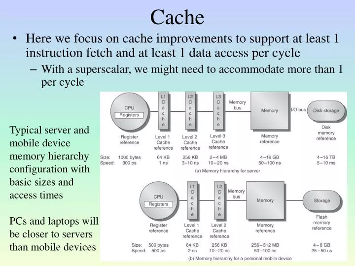
Cache. Here we focus on cache improvements to support at least 1 instruction fetch and at least 1 data access per cycle With a superscalar, we might need to accommodate more than 1 per cycle. Typical server and m obile device memory hierarchy c onfiguration with b asic sizes and

E N D
Cache • Here we focus on cache improvements to support at least 1 instruction fetch and at least 1 data access per cycle • With a superscalar, we might need to accommodate more than 1 per cycle Typical server and mobile device memory hierarchy configuration with basic sizes and access times PCs and laptops will be closer to servers than mobile devices
Performance Formulae • CPU execution time must factor in stalls from memory access • Assume the on-chip cache responds within the amount of time allotted to it from the load/store or instruction fetch unit (e.g., 1 clock cycle) • CPU time = IC * CPI * Clock cycle time • IC * CPI must include all stalls so now we have to add memory stalls • IC * CPI = CPU clock cycles + memory stall cycles • We can view memory cycle stalls as number of stalls per instruction or per memory access (loads & stores have 2 memory accesses per instruction, all others have 1 memory access per instruction) • Memory stall cycles = IC * (misses / instruction) * miss penalty • Memory stall cycles = IC * (memory accesses / instruction) * miss rate * miss penalty • we select the formula based on the data available (some data given in the text is misses / instruction, some is miss rate
Examples • CPI = 1.0 for cache hits • only data accesses are loads and stores • 50% of all instructions are loads/stores • miss penalty = 25 clock cycles • miss rate = .02, how much faster is an ideal machine? • CPU time ideal = IC * 1.0 * clock cycle time • CPU time this machine = IC * (1.0 + 1.50 * .02 * 25) * clock cycle time = IC * 1.75 * clock cycle time • ideal machine is 1.75 times faster (75%) • Alternatively, we are told that the average number of misses per instruction is 3% • CPU time this machine = IC * (1.0 + .03 * 25) CCT = IC * 1.75 * CCT
Cache Questions • Where can a block be placed? • Determined by type of cache (direct-mapped, set associative) • (address) mod (number of blocks in cache/set) • for fully associative, block can be placed anywhere • How is a block found • Again, determined by type of cache • (address) mod (number of blocks in cache/set) • because the cache will have fewer blocks than memory, the address alone is not sufficient, so we also store tags in the cache, the remaining portion of the address after the block # and word # is the tag, so if the tag checks, the item is found, otherwise it is not in the cache (cache miss) • Which block should be replaced on a miss? • Direct-mapped: no choice, associative/set-associative use a replacement strategy (random, LRU, FIFO) • What happens on a write?
Write Strategies • On a write, either we have to also send the datum to memory (and other levels) or mark it as invalid/stale/dirty • Write through – write to both (all) levels at once • drawback – since lower levels take more time to access, if we write to the same block in the near future, that write may stall the processor • Write back – mark the line as dirty so that, when we remove it in the future, we write the whole line back to memory • What do we do on a cache miss that is a write? • Write allocate – write to memory and retrieve the block and load it into cache • No write allocate – write to memory but do not retrieve for the cache • How many misses occur if either 100 nor 200 is in memory given the pattern of accesses to the write using write allocate and using no write allocate? • no write allocate: 4 misses (100, 100, read 200, 100) • write allocate: 2 misses (write 100, read 200) Write [100] Write [100] Read [200] Write [200] Write [100]
Example for(i=1;i<1024;i++) { x[i] = b[i] * y; // S1 c[i] = x[i] + z; // S2 } • Computer uses a fully associative write-back data cache • Block size is 64 bytes • Assume x[1024], b[1024] and c[1024] are all double precision floating point arrays with arrays b and c already in cache • moving x into the cache does not conflict with b or c • x[0] is stored at the beginning of a block • Questions: • how many misses arise with respect to accessing x if the cache uses a no-write allocate policy? • how many misses arise with respect to accessing x if the cache uses a write allocate policy? • redo the question with S2 before statement S1
Solution • Each array stores 1024 doubles, a refill line stores 64 bytes • We can get exactly 8 array elements into each refill line • Miss arises because of accesses to array x • No-write allocate policy means that the write in S1 will not load x into the cache therefore a miss in S1 results in a read miss in S2 • Any read miss will bring in a refill line along with the next 7 array items • so a read miss occurs for 1 in 8 array elements • we will have 1024 / 8 = 128 read misses • any read miss will have previously had a write miss giving us a total of 256 misses • Write allocate policy means that the write miss in S1 loads the line into cache, so we won’t have a corresponding read miss in S2 and therefore will have a total of 128 misses • Reversing the order of S1 and S2 leads to the read miss happening first so no matter which write policy is used, we will have 128 read misses and no write misses
Write Buffer • In order to support write through, we can add a write buffer • In essence, the write buffer caches writes so that, to the CPU, writing to cache is the same as writing to memory (that is, they take place at the same time) • but instead, the writes to memory get temporarily cached • If successive writes occur to the same block, they go to the buffer • only if writes are to different blocks do we send the current write buffer contents to memory • on a cache miss, we can even check the buffer to see if it is storing what we need • Example: we have a 4-word write buffer, in the code below, 512 and 1024 map to the same cache line • SW R3, 512(R0) – write to buffer • LW R1, 1024(R0) – load causes block with 512 to be discarded • LW R2, 512(R0) – datum found in write buffer, small penalty!
Opteron Data Cache • 2 way set associative cache • 512 blocks per set • 64 KBytes • 64 bytes per block • CPU address: 40 bits • 25 bit tag • 9 bit block number • 6 bit byte number • Write back cache, so valid bit (dirty bit) needed • LRU replacement strategy Victim buffer discussed later Tag comparisons MUX to select one block on a tag match
Performance: Unified Versus Split Cache • Recall that we want 2 on-chip caches to support 2 accesses per cycle, 1 instruction, 1 data • What would happen if we had a single, unified cache? • Assume either two 16KB caches or one 32KB cache • Assume 36% loads/stores and a miss penalty of 100 cycles • use the table below which shows misses per 1000 instructions (not miss rate)
Solution • First, convert from misses/instruction to miss rate • For the unified cache, 43.3 misses per 1000 instructions • miss rate 32KB unified = 43.3/1000/(1+.36) = .0318 • For the split caches • miss rate 16KB instruction cache = 3.82/1000/1 = .004 • miss rate 16KB data cache = 40.9/1000/.36 = .114 • overall miss rate = (1/1.36) * .004 + (.36/1.36) * .114 = .0326 • Factor miss rate into formula where any load/store instruction causes a 1 cycle stall if we use the unified cache (because we are also doing an instr fetch) • Split cache memory access time = 1 + .0326 * 100 =4.26 • Unified cache memory access time = 1 + .0318 * 100 + .0318 * .36 * 2 * 100 = 6.47 • Even though the split caches have the worse miss rate, the performance is far better because it does not cause stalls when there is no cache miss
Impact of Associativity • One way to improve (lower) miss rate is to use associativity • With associativity, we get to implement a replacement strategy which in turn should better support locality of reference and result in a lower miss rate • But with associativity, we have a slower cache • So, is it worthwhile? Let’s look at an example • The base machine has a CPI of 1.6, clock cycle time of .35 ns, 128 KB direct mapped cache with 64 words per block and a miss penalty of 65 ns (not cycles) • Assume 1.4 memory references per instruction • If we want to replace the direct-mapped cache with a 2-way set associative cache, it increases clock cycle time by 35%, is it worth it?
Solution • Miss rate direct mapped cache = 2.1% • Miss rate 2-way assoc cache = 1.9% • Average memory access time = Hit time + misses/instruction * miss penalty • Misses/instruction = miss rate * memory accesses per instruction • We also have to compute the miss penalty from ns to clock cycles which is 65 ns / .35 ns / clock cycle = 186 cycles (we have to round this number up) and 65 ns / (.35 ns * 1.35) = 138 for the 2-way set associative cache • CPU time • DM = IC * (1.6 + 2.1% * 1.4 * 186) * .35 ns = IC * 2.47 ns • 2-way = IC * (1.6 + 1.9% * 1.4 * 138) * .35 ns * 1.35 = IC * 2.49 ns • Our direct-mapped cache machine is slightly better
Impact on OOC • In our previous example, we saw that a cache miss resulted in a set number of stalls • This is the case in a pipeline where a cache miss stops the pipeline • But in an out-of-order completion architecture, a cache miss can be somewhat hidden • Our machine is the same as the previous example but with the 35% longer clock cycle (.35 ns * 1.35) • We will use the same direct mapped cache with a 65 ns miss penalty but assume 30% of misses is hidden because of reservation stations • memory stall time reduces from 65 ns to 45.5 ns which gives us 45.5 ns / (.35 * 1.35) ns / cycle = 97 cycles • CPU time = IC * (1.6 + 2.1% * 1.4 * 97) * .35 * 1.35 • = IC * 2.10 ns • a significant improvement over the pipelines
Improving Cache Performance • Average memory access time = hit time + miss rate * miss penalty • To improve cache performance we must attempt to do one or more of the following • reduce hit time • reduce miss rate • reduce miss penalty • We look at techniques for all 3 • Miss penalty is the largest value in the equation so it seems to be the most significant item to improve but in fact little can be done to improve memory response time • We have seen that miss rates are already pretty low, can we improve? • On the other hand, hit time occurs 100% of the time, improving cache access time could have as big an impact
Miss Rates: the 3 C’s • Cache misses can be categorized as • compulsory misses • very first access to a block cannot be in the cache because the process has just begun and there has not been a chance to load any of it into cache • capacity misses • the cache cannot contain all of the blocks needed for the process • conflict misses • the block placement strategy only allows a block to be placed in a certain location in the cache bringing about contention with other blocks for that same location • Some optimizations focus on one particular type of miss • conflict misses are more common in direct-mapped caches and are 0 in fully associative caches • capacity misses are the most common cause of a cache miss • see figure B.8 on page B-24
Larger Block Sizes • A larger block size improves compulsory misses • But larger blocks mean fewer blocks which impact conflict misses • Also, the larger the block size, the longer it takes to retrieve a cache block from memory, so while this might improve miss rate, it has the potential to cause a greater miss penalty • Example: We have a 4KB cache of 16 byte blocks and want to increase block size • Assume memory access takes 80 cycles + 2 cycles per 16 bytes (so 16 byte block size has miss penalty of 82 cycles, but 32 byte block has miss penalty of 84 cycles) • EAT 16-byte blocks = 1 + .0857 * 82 = 8.027 cycles • EAT 32-byte blocks = 1 + .0724 * 84 = 7.082 cycles • see figure B.12 on page B-28 for a comparison of various block sizes on different cache sizes, we see that 32 byte blocks are best for 4K cache and 64 byte blocks are the best for larger caches
Higher Associativity • Cache research points to the “2:1 cache rule of thumb” that says a cache of size N has about the same miss rate as a cache of size N / 2 which has the next higher associativity • Direct-mapped 32KB cache = 2-way set associative 16KB cache = 4-way set associative 8KB cache, etc • Research also indicates that there is no significant improvement over an 8-way set associative cache • this leaves us with the question direct-mapped, 2-way, 4-way or 8-way cache? • we saw earlier that each level of associativity increases cache response time which requires that we increase clock cycle time if this is the L1 cache • Through experimentation, we would choose a Direct-mapped cache if our cache sizes are at least 16KB (see figure B.13 on page B-29 for specific results)
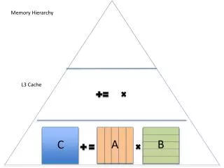
Multi-Level Caches • The on-chip cache must be limited in size but we have room for a large off-chip cache • We can also create a second on-chip cache that is used by multiple cores, so we could wind up with 3 levels of cache • Also, accessing a second or third level cache already causes some delay (stalls) so we could potentially make those caches some form of set associative • this increases the stalls but does not impact clock cycle time • The question of having 2 or 3 levels of cache is based on whether we want to sacrifice room for some cores for a shared cache • The shared cache cannot respond to two cache accesses in the same cycle, so the shared cache’s hit time might vary depending upon if it is currently busy or not
Example: Multi-level Cache Impact • Our EAT formula goes from • Hit time + miss rate * miss penalty to • Hit time1 + miss rate 1 * (hit time 2 + miss rate 2 * miss penalty 2) or • Hit time1 + miss rate 1 * (hit time 2 + miss rate 2 * (hit time 3 + miss rate 3 * miss penalty)) • our L2 cache will duplicate everything in L1 so even though L2 is a much larger cache, its miss rate does not necessarily reflect the difference in size • In fact, the L2 miss rate won’t be nearly as good as the L1 miss rate (usually) • this is L2’s local miss rate (of the number of accesses at L2, how many were misses)? • L2’s global miss rate is the number of misses at L2 / number of total cache accesses which is miss rate 1 * global miss rate 2
Continued • We assume a 16 KB on-chip direct-mapped cache with hit time = 1 clock cycle with a miss rate of 3.94% • A 2nd level on-chip 128 KB 2-way set associative cache with a hit time of 5 clock cycles with a local miss rate of 40% (global miss rate = .016) • A 3rd level off-chip 1MB 8-way set associative cache with a hit time of 10 clock cycles with a local miss rate of 25% (global miss rate = .004) • Memory with a access time of 80 clock cycles • What is the performance with and without the 2nd on-chip cache? • EAT 2 caches = 1 + .0394 * (10 + .25 * 80) = 2.18 cycles • EAT 3 caches = 1 + .0394 * (5 + .40 * (10 + .25 * 80)) = 1.67 cycles
Priority to Read over Write Misses • Reads (loads) occur with a much greater frequency than writes (stores) • Make the common case faster • writes are slower because of the need to write to both cache and main memory and perform the cache tag check prior to starting the write • for a read, the tag check can be done in parallel with the read, the read is canceled if the tag is incorrect • We might use a write buffer for both types of write policy • write-through cache writes to write buffer first, and any read misses are given priority over writing the write buffer to memory • write-back cache writes to write buffer and the write buffer is only written to memory when we are assured of no conflict with a read miss • in either case, a read miss will first examine the write buffer before going on to memory in order to potentially save time
Avoiding Address Translation • The CPU generates a logical address • Whether this is for an instruction or datum • Because of virtual memory, the logical address has to be mapped to a physical address • Look up the page # in the TLB/page table and convert it to a frame # and put together the physical address from it • Unfortunately, this means a second cache access and maybe a memory access if there is a TLB miss • we tuned our system clock to equal 1 cache access, not 2! • One solution: cache instructions and data in the L1 cache using the virtual address instead of the physical address • This has its own problems and solutions, read the text for a complete analysis
Small/Simple L1 Caches • By simple, we mean direct-mapped • This reduces hit time so that our system clock can be faster • set associative and fully associative caches require more hardware for parallel tag comparisons • the direct-mapped cache also has shorter tags • the direct-mapped cache has another advantage, it requires lower power consumption than a set associative cache • Another advantage of the direct-mapped cache is that we can overlap tag check and data access into two cycles • this allows us to create a “super-pipelined” computer where the clock cycle is halved (this is the main difference between MIPS and the MIPS R4000) • we can deepen the overlap to have a greater “cache pipeline” depth, the Intel Core i7 has a 4 cycle pipeline access • The cost of the simple cache is a higher miss rate
Way Prediction • The idea here is to use a 2-way (or greater) associative cache as a direct-mapped cache for greater speed • First, a cache access is started • The cache predicts a “way” • let’s assume a 2-way set associative cache, we predict set 0 or set 1 • We perform the tag comparison based on the prediction and on a hit, we are done (although we might modify any prediction storage) • On a miss, we have a 1 cycle stall while we check the other set’s tag (and possibly revise prediction storage) • On a miss, it’s a true cache miss • Thus our 2-way set associative cache has the miss rate of a 2-way set associative cache and the hit time of a direct-mapped cache on a hit, and a 1 cycle penalty on a miss • Prediction accuracy for a 2-way set associative cache can be as high as 90%
Variation: Pseudo-Associative Cache • Here, we use a direct-mapped cache so we get the direct-mapped hit time • On a cache hit, no change • On a cache miss, invert the last two bits in the line number and check that location • Thus, we have a replacement strategy that lets us place some block, say 101011110 in one of two locations, 101011110 or 101011101 • On a cache miss, we have an extra 1 cycle stall to check the other cache element • In essence, this should give us the same miss rate as the 2-way set associative cache • Which is better, way prediction or pseudo associativity? It comes down to the cost of implementing prediction vs pseudo-associativity
Non-Blocking Caches • When an ordinary cache has a miss and must retrieve the needed block from memory, the cache is unable to respond to other requests • A more expensive cache is a non-blocking cache which can continue to respond to CPU requests while waiting for memory • as long as the new requests are to blocks that are present • this is sometimes referred to as a “hit under miss” • This capability becomes essential for out-of-order execution architectures like Tomasulo’s so that cache does not cause stalls • the result is that part of the miss penalty is hidden because the processor can continue to work in spite of a miss • This is not useful for a pipeline because, when one instruction stalls, later instructions (earlier in the pipeline) should not be allowed to proceed • The non-blocking cache becomes important for implementing some other optimizations which we will see next
Multi-Banked Caches • A common memory optimization is to have multiple memory banks, each of which can be accessed independently • allows parallel access to memory by different devices accessing memory simultaneously or by accessing multiple words of the same block simultaneously (based on the type of interleaving) • We can use this idea on our caches as well by interleaving cache addresses across banks • L2 of AMD Opteron uses 2 banks, Sun Niagara uses 4 banks, ARM Cortex A-8 uses 4 banks and the Intel Core i7 has 4 banks in L1 and 8 in L2 • We will interleave the blocks across banks • for a 4-bank cache, block address % 4 = = 0 would be placed into bank 0, block address % 4 = = 1 would be placed into bank 1, etc • Multiple banks provides us a form of non-blocking cache at a reduced cost
Critical Word First/Early Restart • On a cache miss, an entire block is moved from memory to cache • Part of the miss penalty is the time it takes to access memory and part is the time it takes to move the block over the bus, word-by-word (assuming a 1-word wide data bus) • Rather than having the cache (and CPU) wait until the entire block is available, move the requested word from the block first from memory to cache, and while the rest of the block is being moved, restart the cache access • This optimization requires a non-blocking cache since the cache needs to start responding to the request after the first word is returned • The advantage of this type of cache is that the cache is not waiting for the remaining bus transfers • The miss penalty is now the time for the memory access + 1 bus transfer (recall longer block sizes created larger miss penalties)
Merging Write Buffer • Recall that a write-through cache may use a write buffer to make memory accesses more efficient • the write buffer contains multiple items waiting to be written to memory • with the write buffer, writes to memory are postponed until either the buffer is full or a modified refill line is being discarded • We can make our write buffer more efficient as follows • organize the write buffer in rows, one row represents one refill line • multiple writes to the same line are saved in the same buffer row • a write to memory moves the entire block from the buffer, reducing the number of writes
Compiler Optimizations • Compiler scheduling can improve cache accesses by grouping together accesses of items in the same cache block • Two examples are: • loop interchange:exchange loops in a nested loop situation so that array elements are accessed based on order that they will appear in the cache and not programmer-prescribed order • for(j=0;j<100;j++) • for(i=0;i<5000;i++) • x[i][j] = 2*x[i][j]; • If we invert the two for loops, we match row-major order (the order that the array elements are stored in) and thus greatly improve cache access • blocking executes code on a part of the array before moving on to another part of the array so that array elements do not need to be reloaded into the cache • this is common for applications like image processing where several different passes through a matrix are made • see the example on page 89-90
Hardware Prefetching • Prefetching can be controlled by hardware or compiler (see the next slide) • prefetching can operate on either instructions or data or both • one simple idea for instruction prefetching is that when there is an instruction miss to block i, fetch it and then fetch block i + 1 • this might be controlled by hardware outside of the cache • the second block is left in the instruction stream buffer and not moved into the cache • if an instruction is part of the instruction stream buffer, then the cache access is cancelled (and thus a potential miss is cancelled) • if prefetching is to place multiple blocks into the cache, then the cache must be non-blocking • See figure 2.10 on page 92 which shows the speedup of many SPEC 2000 benchmarks (mostly FP) when hardware prefetching is turned on (speedup ranges from 1.16 to 1.97)
Compiler Pre-fetching • The compiler inserts prefetching instructions into the code (this is for data prefetching only) • Consider the code below, on the left without prefetching causes 150 misses array from a and 101 from b (assuming an 8KB direct-mapped cache with 16 byte blocks, and a and b are double arrays) • The improved code has only 19 misses (see pages 93-94 for the analysis of the misses) • for (j=0;j<100;j=j+1) { prefetch(b[j+7][0]); /* prefetch7 */ prefetch(a[0][j+7]); /* later */ a[0][j]=b[j][0];}; for (i=1;i<3;i=i+1) for (j=0;j<100;j=j+1) { prefetch(a[i][j+7]); a[i][j]=b[j][0]*b[j+1][0]; } • for (i=0;i<3;i=i+1) • for (j=0;j<100;j=j+1) • a[i][j]=b[j][0]*b[j+1][0];
Victim Cache • In a direct mapped cache, consider this situation, assume a cache of 512 entries: • Access to block x • Access to block x + 512 (causes block x to be discarded) • Access to block x • Because the cache must replace block x with x + 512, it results in a miss in the next access • The victim cache is a small, fully associative cache, placed between the cache and memory • this cache might store 1-5 blocks • Victim cache only stores blocks that have been discarded from the cache on a cache miss • On a cache miss, before going to the next level of the hierarchy, check the victim cache first • If we have a hit on the victim cache the block in cache that conflicts with the found block in the victim cache are swapped
Continued • Because the L1 cache is direct-mapped, hit time is still 1, miss rate decreases a little as we are supporting some degree of associativity here • On a cache miss/victim cache hit, this might require more than 2 cycles (1 cycle to visit direct-mapped cache, 2 cycles for the victim cache since its fully associative, 1 additional cycle on a victim cache hit to swap the items