Download
1 / 28
310 likes | 326 Views
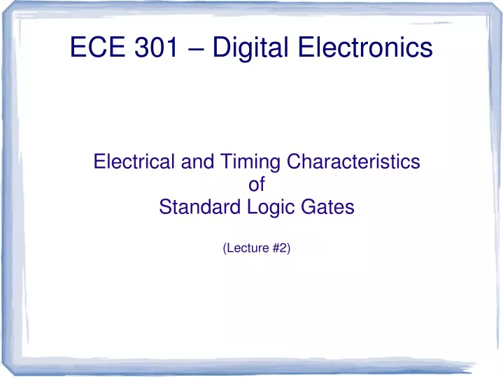
Electrical and Timing Characteristics of Standard Logic Gates (Lecture #2). ECE 301 – Digital Electronics. Standard Logic Gates. Note: “xx” refers to the logic family. Transistor. Logic Family. xx. TTL. Low Power. L. High Speed. H. Schottky. S. Low Power Schottky. LS.

E N D
Electrical and Timing Characteristics of Standard Logic Gates (Lecture #2) ECE 301 – Digital Electronics
ECE 301 - Digital Electronics Standard Logic Gates Note: “xx” refers to the logic family
ECE 301 - Digital Electronics Transistor Logic Family xx TTL Low Power L High Speed H Schottky S Low Power Schottky LS Advanced Schottky AS Adv Low Power Schottky ALS Fast F CMOS High Speed HC Advanced AC Logic Families
ECE 301 - Digital Electronics Comparison of Logic Families
ECE 301 - Digital Electronics (see data sheet for 74LS08) Example: 74LS08
ECE 301 - Digital Electronics (see data sheet for 74HC08) Example: 74HC08
ECE 301 - Digital Electronics Basic Electrical Characteristics
ECE 301 - Digital Electronics Logic Gates • Logic gates are the basic building blocks for (combinational and sequential) logic circuits. • They are, however, abstractions.
ECE 301 - Digital Electronics Logic Gates • In fact, logic gates are electrical circuits.
ECE 301 - Digital Electronics Logic Gates • As such, the logic levels must be represented using an electrical characteristic. • Most technologies use voltages to represent the logic levels. • TTL • CMOS • Some, but very few, technologies use currents to represent the logic levels.
Representing Logic Levels • Ideally, a single voltage value is specified for each logic level. • VDD (power) → Logic 1 • GND (ground) → Logic 0 Logic 1 = high voltage Logic 0 = low voltage
ECE 301 - Digital Electronics Representing Logic Levels • In reality, a range of voltages is specified for each logic level. VDD Logic 1 V1,MIN Undefined Threshold voltages V0,MAX Logic 0 GND
ECE 301 - Digital Electronics Representing Logic Levels • Furthermore, voltage ranges, for logic 1 and logic 0, are specified for both the input and the output of a logic gate. • They are defined in terms of four parameters • VOH = output high voltage VIH = input high voltage • VOL = output low voltage VIL = input low voltage • These are specified in the data sheet for the corresponding logic gate. • They differ from one logic family to another.
ECE 301 - Digital Electronics Output VDD VDD Logic 1 Logic 1 VOH VIH Undefined Undefined VIL VOL Logic 0 Logic 0 GND GND Representing Logic Levels • Input VIH = min. volt. for Logic 1 VOH = min. volt. for Logic 1 VIL = max. volt. for Logic 0 VOL = max. volt. for Logic 0
ECE 301 - Digital Electronics Example: 74LS08 VIH, VIL VOH, VOL
ECE 301 - Digital Electronics Example: 74LS32 VIH, VIL VOH, VOL
ECE 301 - Digital Electronics Example: 74HC32 VIH, VIL VOH, VOL
ECE 301 - Digital Electronics Example: 74LS04 VIH, VIL VOH, VOL
ECE 301 - Digital Electronics Basic Timing Characteristics
ECE 301 - Digital Electronics Time Delay (aka. Latency) • A standard logic gate does not respond to a change on one of its inputs instantaneously. • There is, instead, a finite delay between a change on the input and a change on the output. • The propagation delay of a standard logic gate is defined for two cases: • tPLH = delay for output to change from low to high • tPHL = delay for output to change from high to low
ECE 301 - Digital Electronics low-to-high transition high-to-low transition tPHL tPLH Time Delay
ECE 301 - Digital Electronics Time Delay • The time delay (both tPLH and tPLH) for a logic gate is specified in its data sheet. • The time delay is also known as the • gate delay • propagation delay of the logic gate • latency
ECE 301 - Digital Electronics Example: 74LS08 tPHL, tPLH
ECE 301 - Digital Electronics Example: 74LS32 tPHL, tPLH
ECE 301 - Digital Electronics Example: 74HC32 tPHL, tPLH
ECE 301 - Digital Electronics Example: 74LS04 tPHL, tPLH
ECE 301 - Digital Electronics Time Delay • The propagation delay of a logic circuit can be determined using the time delay of the individual logic gates. • The critical path in the logic circuit must be identified. • The critical path is the path with the greatest delay. • The propagation delay of a logic circuit can be used to define • When the output of the logic circuit is valid. • The maximum speed of a combinational logic circuit. • The maximum frequency of a sequential logic circuit.
ECE 301 - Digital Electronics Questions?