Download
1 / 16
350 likes | 756 Views
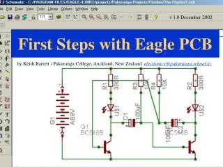
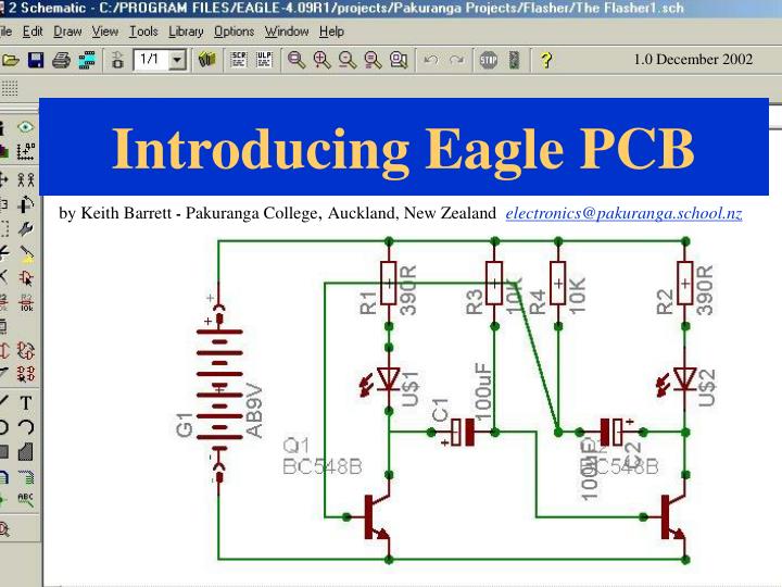
1.0 December 2002. Introducing Eagle PCB. by Keith Barrett - Pakuranga College , Auckland, New Zealand electronics@pakuranga.school.nz. Why use Eagle PCB?.

E N D
1.0 December 2002 Introducing Eagle PCB by Keith Barrett-Pakuranga College, Auckland, New Zealand electronics@pakuranga.school.nz
Why use Eagle PCB? This is a cad package which is available as a freeware version (Eagle lite). Although it may look intimidating at first glance, can be used to produce quality printed circuit boards from circuit schematic diagrams. It is an ideal tool to use for NCET Unit Standards 18242 and 18243. The website from which this software can be downloaded (Windows and Linux versions are available) is www.cadsoft.de
How to use this presentation? It would be useful to have access to two adjacent computers. Install and run Eagle on one and this presentation on the other. . Alternatively, print the pages of this presentation and work through them with Eagle running on your PC. .
Eagle Title Screen This is the control panel screen which should appear when the programme opens.
Directory tree. . . To begin with only focus upon the LIBRARIES and PROJECTS directories Eagle Control Panel
Eagle PCB Libraries Click hereto display the LIBRARIES
These folders contain the data used to generate the symbols for the diagrams. They contain schematic pinout data for individual components and package layout diagrams used on the pcb layout These buttons allow you to select and de-select files. Libraries
Libraries - example This file type contains schematic pinout data This file type contains standard package layout diagrams used on the pcb layout. File content descriptions
Click on a schematic file Symbol used in schematic diagrams Lists of types sizes and shapes! Libraries - Schematic
Click on a package file Component Information (Reference and dimensions) Symbol used in PCB (component layout) diagrams Libraries - Packages
Eagle PCB Projects Click here to display the PROJECTS
The Projects folders are where you place your work. When creating a design there are two main types of file which are generated by the programme .sch (Circuit schematic designs) and .brd (pcb layout boards) Projects
Schematics The schematic window allows the design of circuits like this flip-flop using standard component symbols From this point the pcb can be created on the “board” screen
Boards This is a board produced from the previous schematic. . . The software automatically generated the symbols and pathways from the schematic. All positioning, track widths and pad sizes can be changed by the user.
Text placed on the “bottom layer” is automatically reversed for printing PCB templates from boards The colour scheme can be customised and layers removed so that the track layer can be printed directly onto a transparency to produce a master for photo-etching
End of presentation 1 Click here to go to the next presentation