Download
1 / 30
340 likes | 660 Views
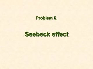
Understanding the Giant Seebeck Coefficient of MnO 2 Nanoparticles . Costel Constantin James Madison University. James Madison University, October 2012. Outline. - Crystal structures and semiconductor properties. - Materials characterization methods.

E N D
Understanding the Giant Seebeck Coefficient of MnO2 Nanoparticles Costel Constantin James Madison University James Madison University, October 2012
Outline • - Crystal structures and semiconductor properties. • - Materials characterization methods. • - Giant Seebeck Coefficient Observed in Manganese Oxide Nanostructures?
unique arrangement of atoms in a crystal. • composed of a unit cell,which is periodically repeated in three dimensions on a lattice. Crystal Structures a = lattice constant WHAT KEEPS THE ATOMS TOGETHER INSIDE OF A CRYSTAL?
IONIC BONDS - electrostatic forces between two oppositely-charged ions, e.g. alkali halogenides • METALLIC BONDS - electrostatic attraction between the metal atoms or ions and the FREE electrons, also called CONDUCTION electrons. e.g. Metals. • COVALENT BONDS - sharing of pairs of electrons between atoms, e.g. Semiconductors, Organic Molecules; C, Si, InSb. • VAN DER WAALS BONDS – arises from the polarization of molecules into dipoles. e.g. Noble Gas crystals, H2, O2. Forces Between Atoms in a Crystal HOW ABOUT THE ENERGY LEVELS IN A CRYSTAL?
Electrons live in ENERGY ORBITALS = ENERGY LEVELS. • ENERGY LEVELS in a crystal, where ions bond, form ENERGY BANDS. Electronic Band Structure in Solids E 3s 3d 3p 2s 2p 1s HOW CAN WE UNDERSTAND THE DIFFERENCE BETWEEN METALS, INSULATORS, AND SEMICONDUCTORS IN TERMS OF ENERGY BANDS?
Define EF as the level below which all electrons fill up the states (little cups). • METALS - Fermi energy level falls at the middle of the allowed band. • INSULATORS and SEMICONDUCTORS - Fermi energy level falls at the middle of the forbidden gap. Metals, Insulators, Semiconductors 3s 3d 3p 2s 2p 1s WHAT IS THE MECHANISM FOR SOME MATERIALS TO CONDUCT ELECTRICITY?
Conduction Bands, Valence Bands, and Band Gaps 3s 3d 3p 2s 2p 1s • VALENCE BAND - created by the outer shell electrons, and most of the states (cups) are occupied by electrons. • CONDUCTION BAND - free electrons coming from VB and able to conduct electricity. • BAND GAP - the width of the forbidden band.
X-ray Diffraction (XRD) • n = integer number for constructive interference. • λ = the wavelength of the incoming and outgoing X-ray. • = the diffraction angle. • Great technique for identifying crystal structures
Seebeck Effect [b] After Thermal Excitation [a] Before Thermal Excitation • Seebeck coefficient, S = - DV/ DT. • Typical values in the order of mV/(o). • It can give an easy carrier type determination for semiconductor substrates.
Scanning Electron Microscope (SEM) and Transmission Electron Microscope (TEM) Fig. 1 Scanning Electron Microscope Fig. 2 Scanning Electron Microscope
Giant Seebeck Coefficient Observed in Manganese Oxide Nanostructures
Why Manganese Oxide Nanoparticles? FangFang Song, Liming Wu and S Liang, Nanotechnology 23, 085401 (2012).
XRD of our as-received MnO2 powder Fig. 1 X-ray diffraction of as-received MnO2 powder Fig. 2 NIST MnO2 standard
Crystal Structure of our Manganese Oxide powder • Rutile structure. • Gray atoms are Mn. • Red Atoms are O. http://en.wikipedia.org/wiki/File:Rutile-unit-cell-3D-balls.png
SEM and TEM images of MnO2 powder Fig. 1 Scanning electron microscope image of MnO2 [ref. 1] Fig. 2 Transmission electron microscopy image of MnO2. 1. FangFangSong, Liming Wu and S Liang, Nanotechnology 23 (2012) 085401 (4pp)
Figure of Merit and Harman Transient Method • Thermoelectric materials are characterized by the figure of merit “ZT”. • Sigma (s) – electrical conductivity. • S – Seebeck coefficient. • Kappa (k) – thermal conductivity. ZT = VDC/VAC - 1
Preliminary Results ZT vs. MnO2 particle stacking density
Preliminary Results Seebeck vs. MnO2 particle stacking density
Preliminary Results Thermal conductivity vs. MnO2 particle stacking density
Conclusions • MnO2nanoparicles are promising for creating devices: Seebeck coefficient can be improved, • conductivity can be improved, and they exhibit very low thermal conductivity. MnO2
Giant Seebeck Coefficient Thermoelectric Device of MnO2 powder
Important Problems to be Studied • How does the Figure of Merit behave as a function of temperature, particule size, and particule density? • By applying the transient Harman method we can find an answer to all these questions. FangFang Song, Liming Wu and S Liang, Nanotechnology 23, 085401 (2012).
Doping Semiconductors • INTRINSIC – do not conduct electricity because electrons are tightly bonded • to the nucleus. • N-type – doping with Phosphorous atoms introduce an extra electron in • the conduction band. • P-type – doping with Boron atoms introduce an extra hole in the conduction band.