Download

1 / 19
190 likes | 322 Views
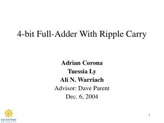
The Compatibility 6 Full-Adder Topologies with V DD Stacking. By Wenlu Sun & Jiyati Verma Thursday, December 1, 2011 ECE 6332 – VLSI Design Final Project Presentation. Overview. Purpose Full Adders Cadence Implementation Simulation Results Takeaways. V DD Stacking.

E N D
The Compatibility 6 Full-Adder Topologies with VDD Stacking By Wenlu Sun & Jiyati Verma Thursday, December 1, 2011 ECE 6332 – VLSI Design Final Project Presentation
Overview • Purpose • Full Adders • Cadence Implementation • Simulation Results • Takeaways
VDD Stacking • Noise Reduction attenuates Power Dissipated …Application of Stacked-VDD to adders
Purpose • To minimize the fluctuation of Vmiddle • Which full adder topology does this the best? Can we make any generalizations in those decisions? Static Dynamic Transmission Gates
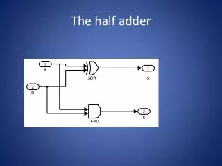
Static Full Adders Static CMOS Mirror Adder
Transmission Logic Adders Transmission Function Adder Transmission Gate Adder
Dynamic NP CMOS Adders Standard Fare (#1) Suggested From a Paper(#2)
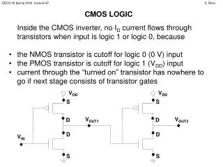
(10) A0 FA0 S0 (01) B0 Cout,0 Cin,0 = A0 + – Vmiddle VDD (01) A1 FA1 S1 (10) B1 Cout,1 Cin,1 = A1 Cadence Implementation Claim: When inputs of FA0 and FA1 swing in opposite directions, then the greatest amount of noise occurs at the output causing the most imbalanced Vmiddle conditions.
Static CMOS Adder • 1.205 to 1.050 V. • Percents: 9.55% above and 4.55% below.
Mirror Full Adder (MFA) • 1.148 to 0.985 V. • Percents: 4.36% above and 10.5% below.
Transmission Function Adder (TFA) • 1.295 to 1.049 V. • Percents: 17.7% above and 4.63% below.
Transmission Gate Adder (TGA) • 1.365 to 0.790 V. • Percents: 24.1% above and 28.2% below.
Dynamic Adder #1 (Dyn1) • 1.335 to 0.7 V • Percents: 21.4% above and 36.4% below.
Dynamic Adder #2 (Dyn2) • 1.406 to 0.861 V • Percents: 27.8% above and 21.7% below.
All together now… • Static CMOS: +9.55%/-4.55% (Avg: 7.05%) • MFA: +4.36%/-10.5% (Avg: 7.43%) • TFA: +17.7%/-4.63% (Avg: 11.2%) • Dyn2: +27.8%/-21.7% (Avg: 24.8%) • TGA: +24.1%/-28.2% (Avg: 26.2%) • Dyn1: +21.4%/-36.4% (Avg: 28.9%)
Takeaways / Conclusion • Static adders are the best! • Dynamic adders compromise stability for speed, which is needed in Stacked-VDDdesigns • Out of transmission logic adders, TFA does the best balancing of current