Download
1 / 43
430 likes | 539 Views
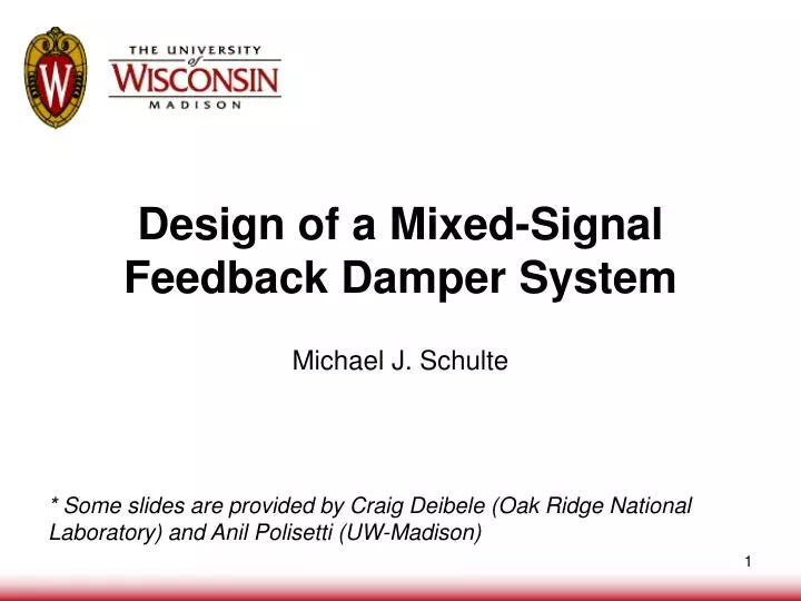
Design of a Mixed-Signal Feedback Damper System. Michael J. Schulte. * Some slides are provided by Craig Deibele (Oak Ridge National Laboratory) and Anil Polisetti (UW-Madison). Project Group. University of Wisconsin, Madison Michael Schulte Anil Polisetti Suman Mamidi Zaipeng Xie

E N D
Design of a Mixed-Signal Feedback Damper System Michael J. Schulte * Some slides are provided by Craig Deibele (Oak Ridge National Laboratory) and Anil Polisetti (UW-Madison)
Project Group • University of Wisconsin, Madison • Michael Schulte • Anil Polisetti • Suman Mamidi • Zaipeng Xie • Oak Ridge National Laboratory • Craig Deibele • Saeed Assadi • Jeffrey Patterson • Los Alamos National Laboratory • Rob McCrady • Bob Macek • Hardware components from Sundance DSP Inc.
Outline • Project Goals and Motivation • System Overview • System Components • Analog-to-digital and digital-to-analog converters • Field programmable gate array (FPGA) modules • System Features • System Status • Future Work and Conclusions
Project Goals and Motivation • Goal: Develop a mixed-signal feedback damper system for use at Oakridge and Los Alamos • Provides • Flexibility in setting system parameters • Programmability to meet the needs of different experiments • Improved data collection and analysis • Ability to correct for dispersion
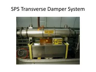
Instability at SNS Frequency spectrum of beam at Spallation Neutron Source
Analog Feedback Damper System pickup kicker • Replace portions of the analog system by digital hardware • Add new functionality and capabilities
Mixed-Signal Damper System • The new system combines analog and digital components • The digital components are clocked at a multiple of the ring frequency (≈ 1 MHz)
Digital Subsystem Implementation • The digital subsystem includes synchronized ADCs, FPGAs, and DACs • Desired operating frequency of roughly 400 MHz • Multiply ring frequency by a factor of about 400 to obtain the system clock
Analog-to-Digital Converter • SMT384 ADC Module • Quad-channel, 125 MSPS, 14-bit ADC • Data interleaving on FPGA provides a 500 MSPS, 14-bit data stream * Figure from Sundance DSP, Inc.
Data Interleaving and Storage FPGA • SMT 398 FPGA Modules • Contains Xilinx Virtex-II Pro FPGA • Interleaves data from ADCs for further processing • Stores up to 8 million 16-bit samples * Figure from Sundance DSP, Inc.
Data Processing FPGA • SMT 368 FPGA Module • Contains Virtex-4 FPGA • Stores up to 4 million 16-bit samples • Processes digital data and sends outputs to DAC * Figure from Sundance DSP, Inc.
Digital-to-Analog Converter • SMT 350 DAC Module • SMT350 Dual-Channel 500 MSPS, 16-bit DAC • Accepts data at 125 MSPS and interpolates by 4 • Later upgrade to a true 500 MSPS, 14-bit DAC • Outputs sent to power amplifiers * Figure from Sundance DSP, Inc.
Data Processing FPGA • The FPGA contains high-speed DSP modules • Each module is programmable and can be bypassed • Input from the ADC and outputs to the DACs are stored in high-speed memory
Programmable Delay Module • Phase between the pickup and kicker must be maintained between -90 and +90 degrees • Programmable delay module controls the overall system delay: • FIFO length can be varied • Additional fine-tuning of the delay is required
Comb Filters • The comb filters dampen the ring frequency harmonics to save power • Comb filter output: • Comb filter frequency response: • tn is set as a multiple of the ring frequency (≈ 1 sec)
Comb Filters • The ring frequency harmonics occur at multiples of roughly 1 MHz • To dampen these harmonics, the clock for the comb filter must be synchronized to the ring frequency
FIR Filters • The FIR filters compute: • Serve as equalizers that correct for dispersion in analog components • Cables have non-uniform magnitude and phase versus frequency • Amplifiers have phase dispersion • Analog hybrids and low-pass filters have magnitude and phase dispersion
Cable Magnitude Dispersion • The cables have magnitude and phase dispersion due to copper and dielectric losses characteristics of the measurement cable (in dB) vs. frequency
Cable Phase Dispersion • The cables have magnitude and phase dispersion due to copper and dielectric losses Phase response of Ideal cable vs. Actual cable
Cable Dispersion • Cable magnitude and phase dispersion is seen in its time domain response Time-domain response of Ideal cable vs. Actual cable
Reducing Cable Dispersion • Find the frequency (S21) characteristics of the cable using a vector network analyzer • Determine the equalizer characteristics that compensate for the cables magnitude and phase dispersion Phase response of idea cable, actual cable and the equalizer versus frequency
Reducing Cable Dispersion • Determine the number of taps and tap values for the equalizer • Run the equalizer in series with the cable to reduce dispersion Comparison of the time-domain responses of an ideal, actual, and de-embedded cable
Reducing Overall Dispersion • The impact of other sources of dispersion in the system can be reduced using similar techniques • FIR filters can be designed to compensate for multiple dispersion sources: Phase spectrum of anti-aliasing LPF with cut-off frequency of 180 MHz
System Status • Digital subsystem (ADCs, FPGAs, DACs) currently under construction by Sundance DSP • Preliminary FPGA subsystem design • Modeled, synthesized, and initial testing • Correct operation of digital components • Operating frequency of roughly 400 MHZ • Simulation model developed using Matlab and DSP System Generator • Technique for compensating for dispersion • Developed for cables • In-progress for other analog components
Future Work • Design and test the FPGA control to set system parameters and filter coefficients • Develop a GUI to enter parameters and filter coefficient • Use the Matlab simulation model and experimental data to refine the design • Test complete digital subsystem (first without and then with the ADCs and DACs) • Test complete system at ORNL • Improve the design based on experimental results • Automate the system for adaptive processing • Hardware/software adjustment of parameter values
Conclusions • The mixed-signal feedback damper system has important benefits • Added flexibility and programmability • Improved data collection and analysis • Reduce dispersion from analog components • It also has significant challenges • Achieving high clock rate on ADCs, FPGAs, and DACs • Generating clocks synchronized to the ring frequency • System integration and testing • Preliminary results look promising and the system has the potential for future upgrades
Mixed-Signal Damper System • The new system combines analog and digital components • The digital components are clocked at a multiple of the ring frequency
Digital Subsystem Implementation • The digital subsystem includes synchronized ADCs, FPGAs, and DACs
Offset and Gain Multipliers • Offset multipliers correct the closed orbit offset • Set M1 and M2, such that is close to zero when the beam is stable • Subtractor provides scaled voltage difference • Gain multiplier controls overall system gain • Implemented using high-speed DSP48 modules
Data Processing FPGA • The FPGA contains high-speed DSP modules • Each module is programmable and can be bypassed • Input from the ADCs and outputs to the DACs are stored in high-speed memory
Alternative Mixed Signal System • The offset multipliers and subtraction can be implemented using analog circuits + Reduces system complexity + May improve accuracy of voltage difference • Introduces additional distortion from analog components • Reduces available diagnostic information
Digital Subsystem Implementation • Implementing the offset multipliers and subtraction using analog circuits + Eliminates one of the ADCs and one of the FPGAs modules • Reduces available diagnostic information, since individual voltages are no longer available
Digital Subsystem • The digital subsystem includes synchronized ADC, FPGA, and DAC modules
External Clock Source • The external clock source is synchronized to a multiple of ring frequency. • For SNS, this is obtained by a multiple of 450. • Ring frequency of SNS 1MHz (approx) • Required clock is 450 MHz (approx)
External Clock Source • Locking the clock is crucial for correct operation • Very important to maintain phase difference between pickup and kicker • Range of phase difference for proper operation of system from -90 to +90 degrees • Phase difference controlled through programmable delay module
External Clock Source • Frequency response of a Comb Filter properly locked to 1MHz
External Clock Source • Frequency response of the same comb filter with an error of 50KHz in the original clock • Leads to an error of 22.5 MHz in the clock to the FPGA.
External Clock Source contd. • Comparison of comb filter outputs.
Programmable delay • Phase difference between Pickup and Kicker between -90 and 90 to maintain negative feedback. • Any change in this phase difference can lead to driving the instabilities instead of damping them. • This phase difference is obtained by varying the delay values.
Comb Filters • Structure of a Comb Filter ,td is a constant, here 1µsec • Used to save power for stable fixed beam offsets
Comb Filter contd. • Need for the Comb Filter Fourier Spectrum of the beam • Major part of spectral power due to ring harmonics. • Notching out ring harmonics will not affect the instabilities.
Comb Filter contd. • Transmission characteristics