Download
1 / 16
160 likes | 318 Views
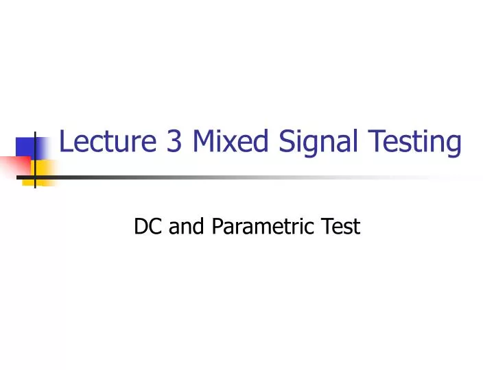
Lecture 3 Mixed Signal Testing. DC and Parametric Test. Continuity Testing. Detect on-chip ESD devices Validate Connection of Device to Tester Eliminate DC Package Bridging Faults 0.1-1.0mA current (over voltage) Parallel testing to speed process Current Limit Test Accuracy.

E N D
Lecture 3 Mixed Signal Testing DC and Parametric Test
Continuity Testing • Detect on-chip ESD devices • Validate Connection of Device to Tester • Eliminate DC Package Bridging Faults • 0.1-1.0mA current (over voltage) • Parallel testing to speed process • Current Limit • Test Accuracy
Power Supply Test: Iddq • Many manufacturing defects result in abnormal power current • Metal Errors – shorted traces • Implant/Diffusion errors – shorted substrate • Faulty ESD Clamps • Open/Floating Wells • Open/Floating Digitial gate input
Power Test II • Testing over Operation Range • (Schmoo Plots): Voltage/Current/Freq • Earliest form of Binning • Memory devices • Processors
Impedance Measurement • Z=V/I (Usually Z=DV/DI) • Force V, measure I (High Impedance) • Force I, Measure V (Low Impedance) • Defined Testing Levels • Reduce possibility of DUT damage • Increase accuracy of measurement
DC Transfer Characteristics • Offset • Input or Output Referenced
Tester Loading Impedance • Input impedance of tester is not infinite • Possibility of substantial error
Output Offset Definition • Single Ended: relative to reference • Differential: • Common Mode (V1+V2)/2 • Differential Mode (V1-V2)
Input Offset • Voltage (Current) needed to set output voltage (current) at reference level • In theory– can measure ouput offset and divide by gain • In practice– gain often too high – device output is pinned to rail
Measuring Gain • For practical Op-Amps, gain is high • Use Nulling amplifier and resistor divider • Null Amplifier acts as servo to drive ouput voltage to known reference • Resistor divider acts to lower input sensitivity • Need Loop Compensation • Want Divider ratio similar to expected Gain • Can get input offset as well by choosing null reference goal
Power Supply Rejection • Input held constant
Common Mode Rejection Ratio • Measure Offset Voltage • Similar problem to Gain – need servo loop
Voltage Search • Need to set input to fix complex output • Three ideas: • Step Search (Ramp) • Issue (Cost of test) • Binary Search (Faster) • Issue (Hysteresis of DUT or Tester) • Linear Search (Simplified form of Newton) • Needs Computerized Tester
Digital DC Tests • Iih/Iil Leakage • Vih/Vil Thresholds • Ioh/Iol Drives • Short Circuit Currents