Download

1 / 11
120 likes | 279 Views
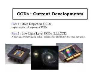
Deep Depletion CCDs. Improving the red response of CCDs. An Introduction Simon Tulloch www.qucam.com. p-type silicon. n-type silicon. Charge Collection in a CCD. Photons entering the CCD create electron-hole pairs. The electrons are then attracted towards

E N D
Deep Depletion CCDs Improving the red response of CCDs. An Introduction Simon Tulloch www.qucam.com
p-type silicon n-type silicon Charge Collection in a CCD. Photons entering the CCD create electron-hole pairs. The electrons are then attracted towards the most positive potential in the device where they create ‘charge packets’. Each packet corresponds to one pixel. pixel boundary pixel boundary incoming photons Electrode Structure Charge packet SiO2 Insulating layer
Electric potential Electric potential Potential along this line shown in graph above. Deep Depletion CCDs 1. The electric field structure in a CCD defines to a large degree its Quantum Efficiency (QE). Consider first a thick frontside illuminated CCD, which has a poor QE. Cross section through a thick frontside illuminated CCD In this region the electric potential gradient is fairly low i.e. the electric field is low. Any photo-electrons created in the region of low electric field stand a much higher chance of recombination and loss. There is only a weak external field to sweep apart the photo-electron and the hole it leaves behind.
Deep Depletion CCDs 2. In a thinned CCD , the field free region is simply etched away. Cross section through a thinned CCD Electric potential Electric potential There is now a high electric field throughout the full depth of the CCD. Thinned CCDs may have good blue response but they become transparent at longer wavelengths; the red response suffers. Problem : This volume is etched away during manufacture Red photons can now pass right through the CCD. Photo-electrons created anywhere throughout the depth of the device will now be detected. Photons no longer have to pass through the electrode structure to reach active silicon.
Deep Depletion CCDs 3. Ideally we require all the benefits of a thinned CCD plus an improved red response. The solution is to use a CCD with an intermediate thickness of about 40mm constructed from Hi-Resistivity silicon. The increased thickness makes the device opaque to red photons. The use of Hi-Resistivity silicon means that there are no field free regions despite the greater thickness. Cross section through a Deep Depletion CCD Electric potential Electric potential Problem : Hi resistivity silicon contains much lower impurity levels than normal. Very few wafer fabrication factories commonly use this material and deep depletion CCDs have to be designed and made to order. Red photons are now absorbed in the thicker bulk of the device. There is now a high electric field throughout the full depth of the CCD. CCDs manufactured in this way are known as Deep depletion CCDs. The name implies that the region of high electric field, also known as the ‘depletion zone’ extends deeply into the device.
100-300 um 40 um Spectral response for differing silicon thickness 16um = standard thinned CCD 40um = E2V Deep Depletion CCD 300um = LBNL SNAP/DEC project CCDs 16 um QE Improvement
QE Improvement QE improvement in detectors at ING EEV12 and TEK4 are standard thinned CCDs. MARCONI2 and MITLL3 use deep depletion silicon
Extra thick Deep Depletion Si. With Deep Depletion Si. Extra thick Deep Depletion Si + Bias Gate Transparent bias gate 40mm 300-600mm -200V LBNL ‘Hi-Rho’ CCDs for SNAP and DEC projects Under thinned standard Si. Electric potential n p Photoelectron lost to recombination Photoelectron detected
LBNL ‘Hi-Rho’ CCDs for SNAP and DEC projects Requires an applied backside potential to ensure good PSF VSUB = 5V 20V 115V
Deep Depletion CCDs 4. Fringing will also be reduced since less light reflects from backside of CCD causing interference Images illuminated by 900nm filter with 2nm bandpass Thinned Marconi CCD >50% fringe amplitude CCID20 Deep Depletion CCD Test data courtesy of ESO
A Cryogenic Deep Depletion Camera CC1D20 2k x 4k x 15mm pixels