Download
1 / 18
190 likes | 494 Views
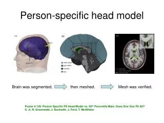
Model-Specific Registers. A look at Intel’s scheme for introducing new CPU features. Test Registers. The 80386 implemented two registers for testing its Translation Look-aside Buffer (i.e., the special cache used for speeding up virtual-to-physical address-conversions

E N D
Model-Specific Registers A look at Intel’s scheme for introducing new CPU features
Test Registers • The 80386 implemented two registers for testing its Translation Look-aside Buffer (i.e., the special cache used for speeding up virtual-to-physical address-conversions • The registers were named TR6 and TR7 • Intel warned that these system registers were unique to the 80386 CPU’s design and might not be present in future chips
Then three more • The TR6 and TR7 registers were kept in the 80486 design -- along with three extra Test Registers (TR3, TR4, TR5) that allowed testing of the processor’s caches for code and data • Again Intel warned that these registers were unique to the 80486 CPU’s design and that they might not be implemented in subsequent chips • Sure enough, in the 80586 (‘Pentium’) they were gone – so software written to use them would no longer execute on the newer Pentium CPUs
The ‘Model-Specific’ concept • Beginning with the Pentium processor, Intel has been including ‘experimental’ features in its processors, warning that they may disappear from future designs, but providing a standard and permanent way for all such features to be accessed • This access is via a pair of ‘privileged’ instructions (rdmsr and wrmsr) that can only be executed by ‘ring0’ code
Quite a few MSRs now! • At first there were only about a dozen of these MSRs (Model-Specific Registers), but lately their number is well over 200 • Some MSRs have evidently proven to be sufficiently satisfactory and worth having that they are now deemed as permanent fixtures of the defined i386 architecture
The Time-Stamp Counter • This 64-bit Model-Specific Register was introduced in the Pentium processor and has been present in each CPU thereafter • It increments once every CPU clock-cycle, starting from 0 when power is turned on • It won’t overflow for at least ten years • Unprivileged programs (ring3) normally can access, it via the rdtsc instruction
Using the TSC 64-bits 63 32 31 0 EDX EAX time0: .quad 0 # saves starting value from the TSC time1: .quad 0 # saves concluding value from TSC # how you can measure CPU clock-cycles in a code-fragment rdtsc # read the Time-Stamp Counter movl %eax, time0+0 # save least-significant longword movl %edx, time0+4 # save most-significant longword # <Your code-fragment to be measured goes here> rdtsc # read the Time-Stamp Counter movl %eax, time1+0 # save least-significant longword movl %edx, time1+4 # save most-significant longword # now subtract starting-value ‘time0’ from ending value ‘time1’
The TSC as an MSR • Each Model-Specific Register has its own identifying register-number, and can be accessed (from ring0) using the special pair of instructions: rdmsr and wrmsr • The Time-Stamp Counter is MSR number 0x10 • To write a new 64-bit value into the TSC, you load the desired 64-bit value into the EDX:EAX register-pair, you put the MSR ID-number 0x10 into register ECX, then you execute wrmsr
IA32_APIC_BASE • This register has MSR number 0x1B and it’s private to each CPU in an SMP system • It establishes the base-address for the Local-APIC’s memory-mapped registers (the default base-address is 0xFEE00000, but that can be changed using this MSR) • The CPU’s Local-APIC functions can be either enabled or disabled (via bit #11) • The BSP can be recognized (via bit #8)
Relocating the APIC registers IA32_APIC_BASE (64-bits) 63 32 31 12 11 8 0 reserved APIC base-address (4K page-number) E N B S P Default-value for APIC base-address page = 0xFEE00 Local-APIC Enable bit (1=enabled, 0=disabled) Boot-Strap Processor (read-only): 1=yes, 0=no # make the processor’s Local-APIC registers accessible in real-mode mov $0x000D8000, %eax # least-significant 32-bits mov $0x00000000, %edx # most-significant 32-bits mov $0x1B, %ecx # MSR register-number wrmsr # write to specified MSR
Extended Feature Enable Register • The EFER was introduced in conformity with Advanced Microprocessor Designs way of implementing 64-bit architecture • Its MSR register-number is 0xC0000080 IA32_EFER (64-bits) 63 32 31 12 11 10 9 8 0 reserved reserved X D 3 2 e A 3 2 e E S Y S C A L L eXecute-Disable bit in paging structures (1=enabled, 0=disabled) IA32e-mode is active (1=yes, 0=no) Enable IA32e-mode (1=yes, 0=no) Enable SYSCALL/SYSRET instructions in 64-bit mode (1=yes, 0=no)
Demo: ‘try64bit.s’ • We created a demo-program that shows what steps are needed to enable the new 64-bit capabilities of recent Pentium-D or Core 2 Duo processors (using EFER) • This demo cannot be executed on our current CS Lab/Classroom workstations, but it CAN execute on a remote-access department server named ‘anchor00’
New 4-Level page-tables needed • For executing in 64-bit mode, the PAE-bit (Page-Addressing Extensions) must be enabled (bit #6 in Control Register CR4) and 4-levels of page-table structures must be prepared which implement an “identity mapping” for the transition-code itself • Then 64-bit mode is entered by turning on the PG-bit in Control Register 0 (assuming bit #8 in the EFER register was set to 1)
4-Levels of mapping 63 48 47 39 38 30 29 21 20 12 11 0 sign-extension PML4 PDPT PDIR PTBL offset Page Frame (4KB) 64-bit ‘canonical’ virtual address Page Table Page Directory Page Directory Pointer Table Page Map Level-4 Table CR3 Each mapping-table contains up to 512 quadword-size entries
Page-Table entry format 63 62 52 51 40 39 32 E X B available reserved (must be 0) Base Address [39..32] 31 12 11 9 8 0 Base Address [31..12] avail G P A T D A P C D P W T S / U R / W P Legend: P = present (0=no, 1=yes) PWT = Page Write-Through (0=no, 1=yes) R/W (0=read-only, 1=writable) PCD = Page Caching Disable (0=no, 1=yes) S/U (0=supervisor-only, 1=user) PAT = Page-Attribute Table-Index A = accessed (0=no, 1=yes) G = Global page (1=yes, 0=no) D = dirty (0=no, 1=yes)
Segment descriptors • Segment-descriptors and gate-descriptors have an enlarged format in 64-bit mode to accommodate the larger-sized addresses • Segment-Limit and Base are disregarded for selectors in registers CS, DS, ES, SS 127 64 63 0 Formerly ‘reserved’ bit is now the ‘L’ bit (it indicates a ‘long’ segment-descriptor G D L A P D P L S TYPE
A few GDT descriptors… .align 16 # octaword-alignment (for optimal access) theGDT: .octa 0x00000000000000000000000000000000 # null .equ sel_cs64, (. – theGDT)+0 # code64 selector (ring0) .octa 0x000000000000000000209A0000000000 # code .equ sel_cs32, (. – theGDT)+0 # code32 selector (ring0) .octa 0x000000000000000000409A010000FFFF # code .equ sel_vram, (. – theGDT)+0 # data16 selector (ring3) .octa 0x00000000000000000080F20B80000007 # data
You must update ‘binutils’ • You cannot assemble and link programs that are written for the IA32e 64-bit mode unless you install the newest versions of the GNU assembler ‘as’ and the linker ‘ld’ • You can download these utilities from the website for the Free Software Foundation at: http://www.fsf.org/ • Directions for installing are easy-to-follow