Download
1 / 19
190 likes | 367 Views
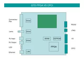
9U FPGA. Implements all D0 specific functions and registers TSI Functions/Registers PIO Registers/MBUS arbitration FIFOs/Mapper Registers/Broadcast arbitration. PMC to 9U Function. PMC sends data (64 bits) + control words (13 bits total) 9U FPGA decodes control word PIO Write/Read

E N D
9U FPGA • Implements all D0 specific functions and registers • TSI Functions/Registers • PIO Registers/MBUS arbitration • FIFOs/Mapper Registers/Broadcast arbitration
PMC to 9U Function • PMC sends data (64 bits) + control words (13 bits total) • 9U FPGA decodes control word • PIO Write/Read • Register setup (PIO/DMA) • TSI Read • ECL Write
Drew and Bob’s Draft #1 • Basic design ideas: • Use any off the shelf SBC • Use generic ~off the shelf pmc interface to PCI • Leave open possibility to upgrade CPU’s • Leave open possibility to support a 64 bit PCI SBC w/o modification to 9u card Mechanical: sbc sits inside of 9u card, If SBC is 1 slot, the whole beta system is 1 slot 9u SBC PMC fpga fifos 64 bit bus
WCK WCK RCK RCK FIFO FIFO WEN WEN REN REN Drew and Bob’s Draft #1 Block Diagram PMC Drivers 64 9u card 13 Control/Arb 64 64 128 Altera 10K100 MBDA MBAD 32 12 To Hlink? MBARB 32 Drivers 12 To Hlink? P2 Lines 16 33 To ECL
Drew and Bob’s Draft #1 Comments: We included new drivers on the PMC and drivers on the 9u card because we expected that the TTL from the fifo’s, FPGA, and PMC might not be able drive the cable. I’m not sure this is a problem after giving it more thought… (more later) The FPGA model here is that the PMC card’s FPGA serves a a bridge between the local bus of the PCI interface and the private used to connect the PMC w/ the FPGA on the 9u card. The 9u FPGA replace the PIO/DMA/ and TSI devices and maybe also provides a new hotlink output. It also supports a custom interface to the PMC card.
Orsay Draft • Basic design ideas: • A single fpga can do the job instead of programming two of them • do away / PMS + cable • do away w/ drivers by keeping signal paths short in this design • Choose one off the shelf SBC • 9u card is layed out to mate w/this board Mechanical: sbc sits under the 9u card. It’s PMC connector plugs into the bottom of the 9u board, the is no PMC card – this eats two slots minimum. 9u SBC Pci controller on 9u card pmc conn 32 bit bus localbus fpga fifos
WCK WCK WCK WCK RCK RCK RCK RCK FIFO FIFO FIFO FIFO WEN WEN WEN WEN REN REN REN REN Orsay Draft Block Diagram AMCC PCI Interface 9u card 32 A/D + Control/Arb PCI interface local bus 32 128 Altera 20K200 MBDA MBAD 32 MBARB 32 Drivers P2 Lines 16 33 To ECL
Orsay Draft Comments: One card to build, all function is on 9u card. No differential drivers used – FIFO output is buffered through FPGA, and bus lengths are kept short ~ 20 cm, to TTL can drive w/ no problems at 33MHz (local bus speed = PCI buss speed) The 9u FPGA replace the PIO/DMA/ and TSI devices and maybe also provides a new hotlink output. It now serves at the local bus interface.
Bob/Drew + use ~any SBC at any time + 64-bit connection from 9u card allows added upgrade path for SBCs + mechanicals similar to standard VME extender board -two FPGA’s to program -two bus protocals -two boards to build (IF the cern card needs new drivers added…) Orsay + one card to build +1 fpga to program +1 local bus protocal +all TTL interface to SBC (no differential drivers) -fixed choice of SBC -essentially no upgrade path w/o major redesign -personal opinion odd mechanicals
Fifo to DMA Arbitration LCLK ~40MHz FIFO MT DMA RDY ADDR AD/DA(0:63) AD DA0 DA1 DA2 DA3 Latch
Replace drivers w/ differential or other suitable variety 64-bits of data have common direction/tristate Other I/O drivers should have individually controllable direction
Add two (very) low profile connectors • FPGA program interface • LA hookup to spare I/O pins of FPGA • PMC must stay within profile height and power consumption restrictions Modernize FPGA: More logic cells + faster clock available in SAME package?
Remove PN3? – what is it’s function Why j-mode? Vs. c-mode? Eeprom? What’s the best way to run a clock between the pmc and 9u, Through drivers like other signals?
DMA Function • 9U-FPGA mapper registers set from PMC • PMC raises READY bit when DMA is possible • 9U-FPGA arbitrates DMA • “” find target address • “” sends target address to PMC and ‘GO’ signal • “” controls FIFO WCLOCK, counts words in broadcast • “” sends RCLOCKS to FIFOs as long as READY is set • “” sends DMA STOP when event is finished
PIO Master (coupled) Write Function • 9U-FPGA mapper registers set from PMC • PMC writes address/data to 9U-FPGA and waits holding PCI bus • 9U-FPGA arbitrates MBUS and writes • 9U-FPGA completes write or times out and sends DONE to PMC • PMC releases PCI bus • Note: we may be able to develop an uncoupled write function • Do we want to add a STATUS register? Write error interrupt?
PIO Slave (coupled) Write Function • 9U-FPGA mapper registers set from PMC • “” responds to MB Master, latches address/data • “” writes address/data to PMC and holds MBUS • “” (optionally halts and FIFO readout in progress) • “” sets up PCI target address in PMC • PMC arbitrates PCI bus and performs (4 x 32-bit) writes • 9U-FPGA completes write to PMC replies to MB Master • 9U-FPGA (resumes DMA if necessary)
PIO Master (coupled) Read Function • 9U-FPGA mapper registers set from PMC • PMC writes address to 9U-FPGA and waits holding PCI bus • 9U-FPGA arbitrates MBUS and sends Read request • 9U-FPGA completes read or times out and replies to PMC • PMC fills internal registers w/ 128 bit word and places data (1 32-bit word) on PCI bus • PMC releases PCI bus • Note: we may be able to develop an uncoupled read function • The other 96 bits would be read on register reads to the PMC (this • is how the alpha works now. It may be possible to have the PMC • initiate a PCI burst write in an uncoupled version of this function
PIO Slave (coupled) Read Function • 9U-FPGA mapper registers set from PMC • “” receives address from MBUS • “” (optionally halts and FIFO readout in progress) • “” sends address and requests data from PMC • “” completes read from PMC and sends data to MBUS • “” (resumes DMA if necessary)
40mm 45mm