Download

1 / 94
990 likes | 1.27k Views
Introduction to 8085. Prathamesh Bhat. 8085 INTRODUCTION. The features of INTEL 8085 are : It is an 8 bit processor. It is a single chip N-MOS device with 40 pins. It has multiplexed address and data bus.(AD 0 -AD 7 ). It works on 5 Volt dc power supply.

E N D
Introduction to 8085 Prathamesh Bhat
8085 INTRODUCTION • The features of INTEL 8085 are : • It is an 8 bit processor. • It is a single chip N-MOS device with 40 pins. • It has multiplexed address and data bus.(AD0-AD7). • It works on 5 Volt dc power supply. • The maximum clock frequency is 3.072 MHz while minimum frequency is 500kHz. • It provides 74 instructions with 5 different addressing modes.
8085 INTRODUCTION • It provides 16 address lines so it can access 2^16 =64K bytes of memory. • It generates 8 bit I/O address so it can access 2^8=256 input ports. • It provides 5 hardware interrupts:TRAP, RST 5.5, RST 6.5, RST 7.5,INTR. • It provides Accumulator,oneflag register ,6 general purpose registers and two special purpose registers(SP,PC). • It provides serial lines SID ,SOD.So serial peripherals can be interfaced with 8085 directly.
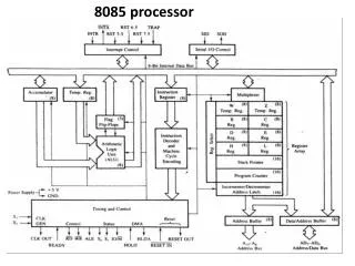
8085 PIN DESCRIPTION Some important pins are : • AD0-AD7: Multiplexed Address and data lines. • A8-A15: Tri-stated higher order address lines. • ALE: Address latch enable is an output signal.It goes high when operation is started by processor . • S0,S1: These are the status signals used to indicate type of operation. • RD¯: Read is active low input signal used to read data from I/O device or memory. • WR¯:Write is an active low output signal used write data on memory or an I/O device.
8085 PIN DESCRIPTION NOTE- µP= Microprocessor • READY:This an output signal used to check the status of output device.If it is low, µP will WAIT until it is high. • TRAP:It is an Edge triggered highest priority , non maskableinterrupt. After TRAP, restart occurs and execution starts from address 0024H. • RST5.5,6.5,7.5:These are maskable interrupts and have low priority than TRAP. • INTR¯&INTA:INTR is a interrupt request signal after which µP generates INTA or interrupt acknowledge signal. • IO/M¯:This is output pin or signal used to indicate whether 8085 is working in I/O mode(IO/M¯=1) or Memory mode(IO/M¯=0 ).
8085 PIN DESCRIPTION • HOLD & HLDA:HOLD is an input signal .When µP receives HOLD signal it completes current machine cycle and stops executing next instruction.In response to HOLD µP generates HLDA that is HOLD Acknowledge signal. • RESET IN¯:This is input signal.WhenRESET IN¯ is low µp restarts and starts executing from location 0000H. • SID: Serial input data is input pin used to accept serial 1 bit data . • X1X2:These are clock input signals and are connected to external LC or RC circuit. These are divide by two so if 6 MHz is connected to X1X2,the operating frequency becomes 3 MHz. • VCC&VSS:Power supply VCC=+ -5Volt& VSS=-GND reference.
Arithmetic and Logical group Accumulator: It is 8 bit general purpose register. • It is connected to ALU. • So most of the operations are done in Acc. Temporary register: It is not available for user • All the arithmetic and logical operations are done in the temporary register but user can’t access it. Flag: It is a group of 5 flip flops used to know status of various operations done. • The Flag Register along with Accumulator is called PSW or Program Status Word.
Arithmetic and Logical group Flag Register is given by: S:Sign flag is set when result of an operation is negative. Z:Zero flag is set when result of an operation is 0. Ac:Auxiliary carry flag is set when there is a carry out of lower nibble or lower four bits of the operation. CY:Carry flag is set when there is carry generated by an operation. P:Parity flag is set when result contains even number of 1’s. Rest are don’t care flip flops.
Register Group • Temporary registers (W,Z):These are not available for user. These are loaded only when there is an operation being performed. • General purpose:There are six general purpose registers in 8085 namely B,C,D,E,H,L.These are used for various data manipulations. • Special purpose :There are two special purpose registers in 8085: • SP :Stack Pointer. • PC:Program Counter.
Register Group Stack Pointer: This is a temporary storage memory 16 bit register. Since there are only 6 general purpose registers, there is a need to reuse them . • Whenever stack is to be used previous values are PUSHED on stack and then after the program is over these values are POPED back. Program Counter: It is 16 bit register used to point the location from which the next instruction is to be fetched. • When a single byte instruction is executed PC is automatically incremented by 1. • Upon reset PC contents are set to 0000H and next instruction is fetched onwards.
INSTRUCTION REGISTER,DECODER & CONTROL • Instruction register:When an instruction is fetched , it is executed in instruction register.This register takes the Opcode value only. • Instruction decoder: It decodes the instruction from instruction register and then to control block. • Timing and control:This is the control section of µP.It accepts clock input .
INTERRUPT CONTROL SERIAL IO CONTROL GROUP • It is used to accept the serial 1 bit data by using SID and SOD signals and it can be performed by using SIM & RIM instructions. • It accepts different interrupts like TRAP INT5.5,6.5,7.5and INTR.
INTERRUPTS IN 8085 • Interrupt is a process where an external device can get the attention of the microprocessor. The process starts from the I/O device The process is asynchronous. • Classification of Interrupts Interrupts can be classified into two types: • Maskable Interrupts (Can be delayed or Rejected) • Non-Maskable Interrupts (Can not be delayed or Rejected)
INTERRUPTS IN 8085 Interrupts can also be classified into: • Vectored (the address of the service routine is hard-wired) • Non-vectored (the address of the service routine needs to be supplied externally by the device) • An interrupt is considered to be an emergency signal that may be serviced. • The Microprocessor may respond to it as soon as possible.
INTERRUPTS IN 8085 • The 8085 has 5 interrupt inputs. • The INTR input. The INTR input is the only non-vectored interrupt. INTR is mask-able using the EI/DI instruction pair. RST 5.5, RST 6.5, RST 7.5 are all automatically vectored. • RST 5.5, RST 6.5, and RST 7.5 are all mask-able. TRAP is the only non-mask-able interrupt in the 8085 • TRAP is also automatically vectored.
INTERRUPTS IN 8085 • Non vectored interrupts: • The 8085 recognizes 8 RESTART instructions: RST0 - RST7 . Each of these would send the execution to a predetermined hard-wired memory location:
TIMING AND STATE DIAGRAM • The µP operates with reference to clock signal.The rise and fall of the pulse of the clock gives one clock cycle. • Each clock cycle is called a T state and a collection of several T states gives a machine cycle. • Important machine cycles are : • Op-code fetch. • Memory read. • Memory write. • I/Op-read. • I/O write.
TIMING AND STATE DIAGRAM Op-code Fetch:It basically requires 4 T states from T1-T4 • The ALE pin goes high at first T state always. • AD0-AD7 are used to fetch OP-code and store the lower byte of Program Counter. • A8-A15 store the higher byte of the Program Counter while IO/M¯ will be low since it is memory related operation. • RD¯ will only be low at the Op-code fetching time. • WR¯ will be at HIGH level since no write operation is done. • S0=1,S1=1 for Op-code fetch cycle.
TIMING AND STATE DIAGRAM Fig referrence- R S Gaonkar Op-code fetch cycle :
TIMING AND STATE DIAGRAM Memory Read Cycle: It basically requires 3T states from T1-T3 . • The ALE pin goes high at first T state always. • AD0-AD7 are used to fetch data from memory and store the lower byte of address. • A8-A15 store the higher byte of the address while IO/M¯ will be low since it is memory related operation. • RD¯ will only be low at the data fetching time. • WR¯ will be at HIGH level since no write operation is done. • S0=0,S1=1 for Memory read cycle.
TIMING AND STATE DIAGRAM Memory write Cycle: It basically requires 3T states from T1-T3 . • The ALE pin goes high at first T state always. • AD0-AD7 are used to fetch data from CPU and store the lower byte of address. • A8-A15 store the higher byte of the address while IO/M¯ will be low since it is memory related operation. • RD¯ will be HIGH since no read operation is done. • WR¯ will be at LOW level only when data fetching is done. • S0=1,S1=0 for Memory write cycle.
8085 Memory Interfacing • Generally µP 8085 can address 64 kB of memory . • Generally EPROMS are used as program memory and RAM as data memory. • We can interface Multiple RAMs and EPROMS to single µP . • Memory interfacing includes 3 steps : • Select the chip. • Identify register. • Enable appropriate buffer.
8085 Memory Interfacing • Example: Interface 2Kbytes of Memory to 8085 with starting address 8000H. Initially we realize that 2K memory requires 11 address lines (2^11=2048). So we use A0-A10 . • Write down A15 –A0
8085 Memory Interfacing • Address lines A0-A10 are used to interface memory while A11,A12,A13,A14,A15 are given to NAND GATE/Decoder to provide an output signal used to select the memory chip CS¯or Chip select input. • MEMR¯ and MEMW¯are given to RD¯and WR¯pins of Memory chip. • Data lines D0-D7 are given to D0-D7 pins of the memory chip. • In this way memory interfacing can be achieved.
8085 Memory Interfacing 3:8 Decoder A15- A11 8085 CS A15-A8 ALE A10- A0 2K Byte Memory Chip AD7-AD0 Latch A7- A0 D7- D0 WR IO/M RD WR RD The diagram of 2k interfacing is shown below:
8085 Memory Interfacing • In this example we saw that some address lines are used for interfacing while others are for decoding/selecting the chip. • It is called absolute decoding. • We sometimes don’t requires that many address lines. So we ignore them. But this may lead to shadowing or multiple address. • This type of decoding is called linear decoding or partial decoding. • In partial decoding wastage of address takes place but it requires less hardware and cost is also less as compared with absolute one.
Questions & Answers • Q1) If the instruction at location F200 “MOV C,B” is being executed, What is the PC value? • Q2) Distinguish between peripheral mapped I/O and memory mapped I/O. • Q3) How does MP know what operation to perform first (MEM RD/WR or I/O RD/WR) • Q4) What is an assembler?
ADDRESSING MODES OF 8085 1) Immediate addressing: Immediate data is transferred to address or register. Example: MVI A,20H. Transfer immediate data 20H to accumulator. Number of bytes: Either 2 or 3 bytes long. 1st byte is opcode. 2nd byte 8 bit data . 3rd byte higher byte data of 16 bytes.
ADDRESSING MODES OF 8085 2) Register addressing: Data is transferred from one register to other. Example: MOV A, C :Transfer data from C register to accumulator. Number of bytes: Only 1 byte long. One byte is opcode.
ADDRESSING MODES OF 8085 3) Direct addressing: • Data is transferred from direct address to other register or vice-versa. Example: LDA C200H .Transfer contents from C200H to Acc. Number of bytes: These are 3 bytes long. 1st byte is opcode. 2nd byte lower address. 3rd byte higher address.
ADDRESSING MODES OF 8085 4) Indirect addressing: • Data is transferred from address pointed by the data in a register to other register or vice-versa. Example: MOV A, M: Move contents from address pointed by M to Acc. Number of bytes: These are 3 bytes long. 1st byte is opcode. 2nd byte lower address. 3rd byte higher address.
ADDRESSING MODES OF 8085 5) Implied addressing: • These doesn’t require any operand. The data is specified in Opcode itself. Example: RAL: Rotate left with carry. No.of Bytes: These are single byte instruction or Opcode only.
Instruction classification • Data transfer • Arithmetic operations • Logical operations • Branching Operations • Machine Control operations
MP operations related to data manipulation can be summarised in four functions. • Copying data • Performing arithmetic operations • Performing logical operations • Testing for a given condition and altering program sequence.
INSTRUCTIONS SET OF 8085 DATA TRANSFER GROUP MOV Rd, Rs.(Move data from Rs to Rd). Above instruction is a 1byte instruction Example: MOV C,B. Move the content of register B to C. Initially After execution B=10H. B=10H. C=20H. C=10H. Flags Affected :No flags affected. Addressing mode: Register.
DATA TRANSFER GROUP MVI R, Data.(Move Immediate data to Register). Example: MVI B, 30H. (Move the data 30 H to Register B) Initially After execution B=40H B=30H Flags Affected :No flags affected. Addressing mode: Immediate. The above instruction is a 2byte instruction.
DATA TRANSFER GROUP MOV Rd, M (Move data from Memory to Rd). Example: MOV C,M. Move the content of Memory i.e. “H or L” to C. Suppose the Data at memory pointed By HL pair at C200H is 10H. Initially After execution H=C2,L=00,C=30H H=C2,L=00,C=10H. Flags Affected :No flags affected. Addressing mode: Indirect. 3byte instruction
DATA TRANSFER GROUP LXI Rp,16 bit .(Load 16 bit data to Register pair Immediate). Example: LXI SP, C200H. (Load Stack pointer with C200H). Initially After execution SP=C800H SP=C200H. Flags Affected :No flags affected. Eg. LXI H, F200H Addressing mode: Immediate. 3byte instruction
DATA TRANSFER GROUP STA address.(Store Acc data to address). Example: STA C200H. (Move the data from Acc to C200H). Suppose in Acc the data is 10H. Initially After execution A=10H, C200=20H C200=10H , A=10H Flags Affected :No flags affected. Addressing mode: Direct. 3byte instruction
DATA TRANSFER GROUP LHLD address.(Load HL pair with data from address). Example: LHLD C200H. (Move the data from C200 to HL pair). Suppose at C200 the data is 20H,30H . Initially After execution H=10H,L=20H H=20H,L=30H. C2=20H,00=30H C2=20H,00=30H Flags Affected :No flags affected. Addressing mode: Direct.
DATA TRANSFER GROUP • XCHG (Exchange the data from HL pair to DE pair) Example : XCHG Initially After execution H=20H,L=30H, H=40H,L=70H. D=40H,E=70H. D=20H,E=30H. Flags Affected :No flags affected. Addressing mode: Register.
DATA TRANSFER GROUP IN 8 bit address (Move the data from address to Acc) Example: IN 80H Move the data from 80H port address to Accumulator. Suppose data at 80H is 39H. Initially After execution A=20H. A=39H Flags Affected :No flags affected. Addressing mode: Direct.
DATA TRANSFER GROUP OUT 8 bit address (Move the data from Acc to address) Example: OUT 80H Move the data from Acc to port address 80H. Suppose data at Acc is 39H. Initially After execution A=39H. 80=10H. A=39H,80=39H. Flags Affected :No flags affected. Addressing mode: Direct.
DATA TRANSFER GROUP • Example: Write a program to exchange contents of memory location D000H to D001H LDA D000H Load Acc with data from D000 MOV B,A Move the data to B LDA D0001H Load Acc with data from D001 STA 2000H Store Acc data at D000 MOV A,B Move B’s data to A STA 2001H Store data from D000 to 2001 RST1 Stop.
ARITHMETIC GROUP ADD R (ADD register content with Acc and result in A ). Example: ADD C. (ADD the content of C with A). Suppose the Data at C register is 10H. Initially After execution C= 10H ,A=10H A=20H,C=10H. Flags Affected :All flags are modified. Addressing mode: Register
ARITHMEIC GROUP ADD M(ADD H or L Reg content with Acc and result in A ). Example: ADD M. (ADD the content of HL with A). • Suppose the Data at memory pointed by HL register 1020H is 10H. Initially After execution H= 10H ,L=20H. H=10H,L=20H. A=20H,C=10H. A=30H. Flags Affected :All flags are modified. Addressing mode: Register Indirect.