Download
1 / 20
490 likes | 1.51k Views
Chapter 1 The Crystal Structure of Solids. Describe three classifications of solids—amorphous, polycrystalline, and single crystal. Discuss the concept of a unit cell. Describe three simple crystal structures and determine the volume and surface density of atoms in each structure.

E N D
Chapter 1The Crystal Structure of Solids Describe three classifications of solids—amorphous, polycrystalline, and single crystal. Discuss the concept of a unit cell. Describe three simple crystal structures and determine the volume and surface density of atoms in each structure. Describe the diamond crystal structure. Briefly discuss several methods of forming single-crystal semiconductor materials.
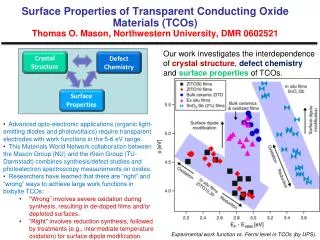
Figure 2.1. Typical range of conductivities for insulators, semiconductors, and conductors. 光電特性 Si is abundant and has very good SiO2 Semiconductor is promising due to high sensitivity in ρ
1.2 TYPES OF SOLIDS The advantage of a single-crystal material is that, in general, its electrical properties are superior to those of a nonsingle-crystal material, since grain boundaries tend to degrade the electrical characteristics.
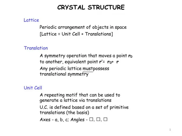
1.3 SPACE LATTICES • The periodic arrangement of atoms in the crystal is called the lattice. • 1.3.1 Primitive and Unit Cell • represent a particular atomic array by a dot that is called a lattice point. • A unit cell is a small volume of the crystal that can be used to reproduce the entire crystal.
A primitive cell is the smallest unit cell that can be repeated to form the lattice.
1.3.2 Basic Crystal Structures • The lattice constant of each unit cell in Figure 1.5 is designated as “a.” • The simple cubic (sc) structure has an atom located at each corner; • the body-centered cubic (bcc) structure has an additional atom at the center of the cube; • the face-centered cubic (fcc) structure has additional atoms on each face plane.
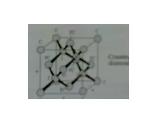
1.4 THE DIAMOND STRUCTURE • Si, Geare referred to as a group IV element and has a diamond crystal structure. • This structure is basically a body-centered cubic with four of the corner atoms missing.
Figure 1.13a shows two body-centered cubic, or tetrahedral, structures diagonally adjacent to each other. The zincblende(sphalerite) structure differs from the diamond structure only in that there are two different types of atoms in the lattice. Compound semiconductors, such as gallium arsenide, have the zinc- blende structure shown in Figure 1.14.
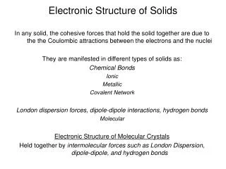
1.5 | ATOMIC BONDING • These oppositely charged ions then experience a coulomb attraction and form a bond referred to as an ionic bond. • Another atomic bond that tends to achieve closed-valence energy shells is covalent bonding • The third major atomic bonding scheme is referred to as metallic bonding. • A fourth type of atomic bond, called the Van der Waals bond, is the weakest of the chemical bonds.
*1.6 | IMPERFECTIONS AND IMPURITIES IN SOLIDS 1.6.1 Imperfections in Solids The thermal energy causes the atoms to vibrate in a random manner about an equilibrium lattice point. This random thermal motion causes the distance between atoms to randomly fluctuate, slightly disrupting the perfect geometric arrangement of atoms. This imperfection, called lattice vibrations Another type of defect is called a point defect. In a real crystal, an atom may be missing from a particular lattice site. This defect is referred to as a vacancy In another situation, an atom may be located between lattice sites. This defect is referred to as an interstitial
A line defect, for example, occurs when an entire row of atoms is missing from its normal lattice site. This de- fect is referred to as a line dislocation
1.6.2 Impurities in Solids • Impurity atoms may be located at normal lattice sites, in which case they are called substitutional impurities. • Impurity atoms may also be located between normal sites, in which case they are called interstitial impurities. • The technique of adding impurity atoms to a semiconductor material in order to change its conductivity is called doping. There are two general methods of doping: impurity diffusion and ion implantation.
*1.7 | GROWTH OF SEMICONDUCTOR MATERIALS 1.7.1 Growth from a Melt A common technique for growing single-crystal materials is called the Czochralskimethod.
1.7.2 Epitaxial Growth • Epitaxial growth is a process whereby a thin, single-crystal layer of material is grown on the surface of a single-crystal substrate. • When grown on the same material, homoepitaxy. • heteroepitaxy, the substrate and epitaxial materials are not the same • One epitaxial growth technique that has been used extensively is called chemical vapor-phase deposition (CVD). • Liquid-phase epitaxyis another epitaxial growth technique. • A versatile technique for growing epitaxial layers is the molecular beam epitaxy (MBE) process.