Download
1 / 16
160 likes | 377 Views
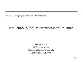
ECE 424 Design of Microprocessor-Based Systems. Hardware Detail of Intel 8088. Haibo Wang ECE Department Southern Illinois University Carbondale, IL 62901. GND. VCC. 1. 40. A14. A15. 2. 39. A13. A16 / S3. 3. 38. A12. A17 / S4. 4. 37. A11. A18 / S5. 5. 36. A10.

E N D
ECE 424 Design of Microprocessor-Based Systems Hardware Detail of Intel 8088 Haibo Wang ECE Department Southern Illinois University Carbondale, IL 62901
GND VCC 1 40 A14 A15 2 39 A13 A16 / S3 3 38 A12 A17 / S4 4 37 A11 A18 / S5 5 36 A10 A19 / S6 6 35 A9 SS0 (High) 7 34 A8 MN / MX 8 33 AD7 RD 9 32 AD6 HOLD (RQ / GT0) 10 31 AD5 HLDA (RQ / GT1) 11 30 AD4 WR (LOCK) 12 29 AD3 IO / M (S2) 13 28 AD2 DT / R (S1) 14 27 AD1 DEN (S0) 15 26 AD0 ALE (QS0) 16 25 NMI INTA (QS1) 17 24 INTR TEST 18 23 CLK READY 19 22 GND RESET 20 21 8088 Pin Configuration
8088 Pin Description Pin Name Pin Number Description Direction GND: 1 & 20 Both need to be connected to ground VCC: 21 VCC = 5V CLK: 19 Input 33% duty cycle 2/3*T 1/3*T MN/MX: 33 Input High Minimum mode Low Maximum mode RESET: 21 Input Reset 8088 • Duration of logic high must be greater than 4*T • After reset, 8088 fetches instructions starting from memory address FFFF0H
8088 READY Selected memoryor I/O device READY Data bus wait for memoryor I/O ready Start data transfer 8088 Pin Description Pin Name Pin Number Description Direction READY 22 Input Informs the processor that the selected memory or I/O device is ready for a data transfer
HOLD 8088 Device 2 HLDA Bus Memory 8088 Pin Description Pin Name Pin Number Description Direction HOLD 31 Input The execution of the processor is suspended as long as HOLD is high HLDA 30 Output Acknowledges that the processor is suspended • Procedure for Device 2 to use bus • Drive the HOLD signal of 8088 high • Wait for the HLDA signal of 8088 becoming high • Now, Device2 can send data to bus
INTR INTR 8088 INTA External device INTA Data Bus Int. type Data bus 8088 Pin Description Pin Name Pin Number Description Direction NMI 17 Input Causes a non-maskable type-2 interrupt INTR 18 Input Indicates a maskable interrupt request INTA 24 Output Indicates that the processor has received anINTR request and is beginning interruptprocessing • NMI (non-maskable interrupt): a rising edge on NMI causes a type-2 interrupt • INTR: logic high on INTR poses an interrupt request. However, this request can be masked by IF (Interrupt enable Flag). The type of interrupt caused by INTR is read from data bus • INTA: control when the interrupt type should be loaded onto the data bus
D Q G 8088 Pin Description Pin Name Pin Number Description Direction ALE 25 Output Indicates the current data on 8088 address/data bus are address A[19:8] Buffer A[19:8] ATE 8088 A[7:0] AD[7:0] D latches D[7:0]
8088 Pin Description Pin Name Pin Number Description Direction DEN 26 Output Disconnects data bus connection DT / R 27 Output Indicates the direction of data transfer DEN DT/R 1 X Disconnected 0 0 To 8088 0 1 From 8088 DEN 8088 DT/R D[7:0] Data bus DEN DT/ R AD[7:0]
8088 Pin Description Pin Name Pin Number Description Direction WR 29 Output Indicates that the processor is writing to memory or I/O devices RD 32 Output Indicates that the processor is reading from memory or I/O devices IO/ M 28 Output Indicates that the processor is accessing whethermemory (IO/M=0) or I/O devices (IO/M=1) WE WR or RD WR OE I/O RD Addr. Dec. CS Addr. Dec. Memory IO/M IO/M 8088
8088 Pin Description Pin Name Pin Number Description Direction AD[7:0] 9-16 I/O Address / Data bus A[19:8] 2-8, 35-39 Input Address bus SS0 34 Output Status Output TEST 23 Input It is examined by processor testing instructions
8284 Clock Generator 8284 8088 RDY1 Ready1 Ready2 RDY2 Ready Ready X1 510 CLK CLK X2 510 +5V RESET RESET RES 100K • Generates 33% duty cycle clock signal • Generates RESET signal • Synchronizes ready signals from memory and I/O devices 10uF
System Timing Diagrams • T-State: • One clock period is referred to as a T-State T-State • An operation takes an integer number of T-States • CPU Bus Cycle: • A bus cycle consists of 4 or more T-States T1 T2 T3 T4
Memory Read Timing Diagrams T3 T4 T2 T1 CLK A[15:8] ALE Buffer A[15:0] 8088 A[19:16] A[19:16] S3-S6 AD[7:0] A[15:8] A[15:8] D latch Memory AD[7:0] A[7:0] D[7:0] IO/M D[7:0] Trans -ceiver DT/R DT/R DEN DEN IO/M RD WR RD WR
Memory Write Timing Diagrams T3 T4 T2 T1 CLK A[15:8] ALE Buffer A[15:0] 8088 A[19:16] A[19:16] S3-S6 AD[7:0] A[15:8] A[15:8] D latch Memory AD[7:0] A[7:0] D[7:0] IO/M D[7:0] Trans -ceiver DT/R DT/R DEN DEN IO/M RD WR RD WR
INTR 8088 External device INTA Data bus Interrupt Acknowledge Timing Diagrams T3 T4 T2 T1 CLK ••• INTR ••• INTA D[7:0] ••• Int. Type • It takes one bus cycle to perform an interrupt acknowledge • During T1, the process tri-states the address bus • During T2, INTA is pulled low and remains low until it becomes inactive in T4 • The interrupting devices places an 8-bit interrupt type during INTA is active
HOLD 8088 Device 2 HLDA Bus Memory HOLD/HLDA Timing Diagrams T2 T3 T4 CLK ••• HOLD ••• HLDA Hold State • The processor will examine HOLD signal at every rising clock edge • If HOLD=1, the processor will pull HLDA high at the end of T4 state (end of the execution of the current instruction) and suspend its normal operation • If HOLD=0, the processor will pull down HLDA at the falling clock edge and resume its normal operation