Download
1 / 18
180 likes | 451 Views
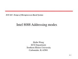
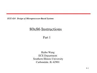
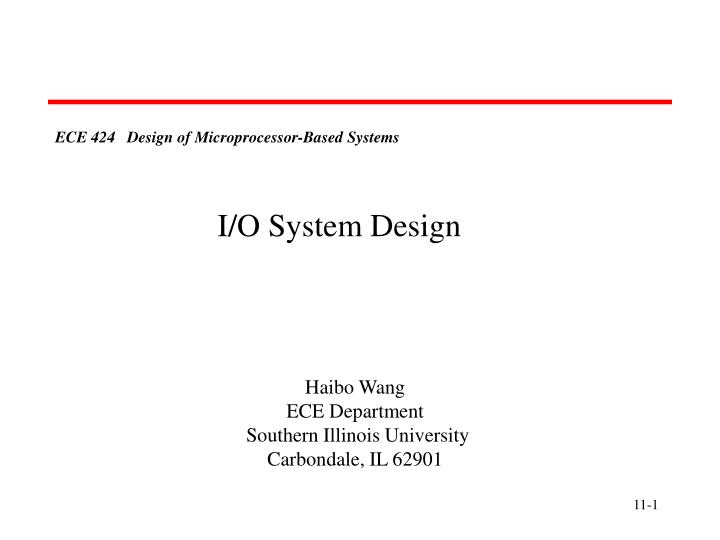
ECE 424 Design of Microprocessor-Based Systems. I/O System Design. Haibo Wang ECE Department Southern Illinois University Carbondale, IL 62901. Data bus. AL. AX. I/O. I/O. I/O. 8088. Address bus A[15:0]. Overview of 8088 I/O System. 65,536 possible I/O ports.

E N D
ECE 424 Design of Microprocessor-Based Systems I/O System Design Haibo Wang ECE Department Southern Illinois University Carbondale, IL 62901
Data bus AL AX I/O I/O I/O 8088 Address bus A[15:0] Overview of 8088 I/O System • 65,536 possible I/O ports • Data transfer between ports and the processor is over data bus • 8088 uses address bus A[15:0] to locate an I/O port • AL (or AX) is the processor register that takes input data (or provide output data)
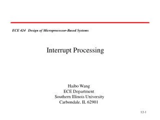
8088 Port Addressing Space • Addressing Space • Accessing directly by instructions IN AL, 80H IN AX, 6H OUT 3CH, AL OUT 0A0H, AX FFFF • Accessing through DX Accessed through DX IN AL, DX IN AX, DX OUT DX, AL OUT DX, AX 00FF Accessed directly by instructions 00F8 0000
Input Port Implementation Data Bus Gating device Input 8088 Address bus Decoder Other control signals • The outputs of the gating device are high impedance when the processor is not accessing the input port • When the processor is accessing the input port, the gating device transfers input data to CPU data bus • The decoding circuit controls when the gating device has high impedance output and when it transfers input data to data bus
A7 Tri-state buffer A6 Data bus Input data A5 A4 A3 CE A2 A1 A0 RD IO/M Input Port Implementation • Circuit Implementation • Assume that the address of the input port is 9CH
A7 A6 Data bus Latch Output data A5 A4 A3 CLK A2 A1 A0 WR IO/M Output Port Implementation • Circuit Implementation • Assume that the address of the output port is 9CH
R A=B B3 A7 A3 B2 A2 A6 B1 A5 A1 B0 A4 A0 A=B A=B B3 A3 A3 B2 A2 A2 B1 A1 A1 B0 A0 A0 A=B RD or WR IO/M A Reconfigurable Port Decoder 1 Vcc
Direct I/O v.s. Memory-Mapped I/O FFFFF FFFFF Memory addressing space I/O FFFF I/O addressing space Memory addressing space 00000 00000 0000 Memory-mapped I/O Direct I/O • Direct I/O: I/O addresses are separated from memory address • Advantage: Do not take memory addressing space • Disadvantage: Use only AL or AX transferring data • Memory-mapped I/O: I/O ports are treated as memory locations • Advantage: Accessing I/O ports is like accessing memory locations Can use other instructions to access I/O ports • Disadvantage: Take memory addressing space
Data bus D[7:0] PA[7:0] A0 8088 PB[7:0] A1 RD Control port WR PC[7:0] RESET A7 CS A6 A5 A4 A3 A2 Port IO/M A1 A0 • 0 0 • 0 1 • 0 • 1 1 PA PB PC Control 8255 Programmable Peripheral Interface
7 6 5 4 3 2 1 0 Command register Port C (C4-C7) Mode select A Port B 0: out 1: in 0: out 1: in 00: mode 0 01: mode 1 1x: mode 2 Port C (C0-C3) Mode set flag Mode select B Port A 0: out 1: in 0: out 1: in 0: mode 0 1: mode 1 0: disabled 1: enabled Programming 8255 • 8255 has three operation modes: mode 0, mode 1, and mode 2
PA[7:0] PA[7:0] PC4 STBA PC7 OBFA PC5 IBFA PC6 ACKA PC3 INTRA PC3 INTRA 8255 8255 PB[7:0] PB[7:0] PC2 STBB PC2 OBFB PC1 IBFB PC1 ACKB PC0 INTRB PC0 INTRB PC6, 7 PC4, 5 Programming 8255 • Mode 0: • Ports A, B, and C can be individually programmed as input or output ports • Port C is divided into two 4-bit ports which are independent from each other • Mode 1: • Ports A and B are programmed as input or output ports • Port C is used for handshaking
PA[7:0] PC7 OBFA PC6 ACKA PC4 STBA PC5 IBFA 8255 PC3 INTRA PC0 In Out In Out In Out STBB OBFB IBFB ACKB INTRB INTRB PC0 PC0 PB[7:0] Mode 1 Mode 0 Programming 8255 • Mode 2: • Port A is programmed to be bi-directional • Port C is for handshaking • Port B can be either input or output in mode 0 or mode 1 • Can you design a decoder for an 8255 chip such that its base address is 40H? • Write the instructions that set 8255 into mode 0, port A as input, port B as output, PC0-PC3 as input, PC4-PC7 as output ?
Start bit B0 B1 B2 B3 B4 B5 B6 Stop bits Parity Serial Data Transfer • Asynchronous v.s. Synchronous • Asynchronous transfer does not require clock signal. However, it transfers extra bits (start bits and stop bits) during data communication • Synchronous transfer does not transfer extra bits. However, it requires clock signal Frame data Asynchronous Data transfer clk Synchronous Data transfer data B0 B1 B2 B3 B4 B5
8251 RS232 D[7:0] TxD RD RD RxD WR WR A0 C/D TxC CLK CLK RxC A7 A6 A5 A4 A3 A2 A1 IO/M 8251 USART Interface
7 6 5 4 3 2 1 0 Mode register Number of Stop bits Baud Rate Parity enable 0: disable 1: enable 00: Syn. Mode 01: x1 clock 10: x16 clock 11: x64 clock 00: invalid 01: 1 bit 10: 1.5 bits 11: 2 bits Character length 00: 5 bits 01: 6 bits 10: 7 bits 11: 8 bits Parity 0: odd 1: even Programming 8251 • 8251 mode register
Programming 8251 • 8251 command register EH IR RTS ER SBRK RxE DTR TxE command register TxE: transmit enable DTR: data terminal ready RxE: receiver enable SBPRK: send break character ER: error reset RTS: request to send IR: internal reset EH: enter hunt mode
DSR SYNDET FE OE PE TxEMPTY RxRDY TxRDY Programming 8251 • 8251 status register status register TxRDY: transmit ready RxRDY: receiver ready TxEMPTY: transmitter empty PE: parity error OE: overrun error FE: framing error SYNDET: sync. character detected DSR: data set ready
Read • Write start start Check RxRDY Check TxRDY No No Is it logic 1? Is it logic 1? Yes Yes Read data register* Write data register* end end * This clears RxRDY * This clears TxRDY Simple Serial I/O Procedures