Download
1 / 37
370 likes | 702 Views
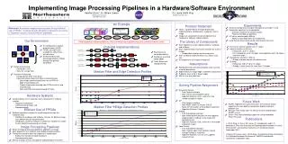
3D FPGA- MEANDER. Abhishek Pandey Reconfigurable Computing ECE 506. Outline:. Introduction TPR Vs MEANDER Methodology Flowchart Partitioning Placement and routing 3D Power Comparison of different 3D tools Results Future Work. Introduction:.

E N D
3D FPGA- MEANDER AbhishekPandey Reconfigurable Computing ECE 506
Outline: • Introduction • TPR Vs MEANDER • Methodology • Flowchart • Partitioning • Placement and routing • 3D Power • Comparison of different 3D tools • Results • Future Work
Introduction: • Better performance per unit area. Limited silicon area and chip size. • Improvement over existing 2D technology • Need better CAD tools to exploit full benefit of 3D FPGA. • 3D as a improvement over FPGA and its limitation
Drawbacks of TPR: • First Synthesizer of 3D FPGA. • All SB’s are assumed 3D • Number of available TSV’s are assumed unlimited. • Area situation becomes worse in 3D FPGA.
Methodology(The electrical equivalent circuit for modeling a TSV):
Flowchart(MEANDER framework): • 3D Partitioning ( 3DPART) • 3D Placement and Routing(3DPRO) • 3D Power( 3DPOWER)
Qualitative comparison between TPR and our proposed solution*: • S. Das, A. Chandrakasan and R. Reif, “Timing, Energy, and Thermal Performance of Three Dimensional Integrated Circuits”, Proceedings of the ACM Great Lakes Symposium on VLSI,(2004), pp. 338-343. Developed at MIT • Kostas Siozios, AlexandrosBartzas, and DimitriosSoudris, “Architecture-Level Exploration of Alternative Interconnection Schemes Targeting 3D FPGAs: A Software-Supported Methodology,” International Journal of Reconfigurable Computing, vol. 2008, Article ID 764942, 18 pages, 2008. doi:10.1155/2008/764942. Developed at National Technical University of Athens (NTUA)
Average variation of application’s delay for a number of layers and TSVs with different electric characteristics:
Average variation of power consumption for a number of layers and TSVs with different electric characteristics:
Experimental setup: • The 3D architectures consist of up to five functional layers. • The hardware resources of each functional layer are identical. • The percentage of vertical interconnects (i.e., TSVs) per functional layer ranges from 10% up to 100%, with a step of 10%. • Each 3D SB realizes four vertical connections. • The electrical parameters for each TSV correspond to fabrication technologies for 3D ICs found in relevant references
Experimental setup: • The 3D architectures consist of up to five functional layers. • The hardware resources of each functional layer are identical. • The percentage of vertical interconnects (i.e., TSVs) per functional layer ranges from 10% up to 100%, with a step of 10%. • Each 3D SB realizes four vertical connections. • The electrical parameters for each TSV correspond to fabrication technologies for 3D ICs found in relevant references
Results(Average Energy×Delay Product (EDP) for different number of functional layers and percentage of fabricated TSVs):
Results(Average wirelength over the MCNC benchmarks for different number of functional layers and percentage of fabricated TSVs):
Results(Average operation frequency over the MCNC benchmarks for different number of layers and percentages of fabricated TSVs):
Results(Average power consumption over the MCNC benchmarks for different number of functional layers and percentage of fabricated TSVs):
Results(Comparison results between 20 biggest MCNC benchmarks: via utilization in 3D FPGA architecture):
Future work: • Experimenting on working with different technology on different layers. • Better CAD tools for 3D FPGAs. • More work need to be done on switch box layout for combination of 2D and 3D switches. • More research need to be done on making better connection within a switch box. • Specialized 3D P & R methods need to be researched.
Conclusion: • A systematic software-supported methodology for exploring and evaluating alternative interconnection schemes for 3D FPGAs is presented. • The methodology is supported by three new CAD tools (part of the 3D MEANDER Design Framework). • The evaluation results prove that it is possible to design 3D FPGAs with limited number of vertical connections without any penalty in performance or power consumption. • More specifically, for the 20 biggest MCNC benchmarks, the average gains in operation frequency, total wirelength, and energy consumption are 35%, 13%, and 32%, respectively, compared to existing 2D FPGAs with identical logic resources.