Download
1 / 2
20 likes | 134 Views
_. [110]. Interface Atomic Structure of Annealed Fe/GaAs(001) Chris J. Palmstrøm (UMN/UCSB) DMR 0913561/0606245.

E N D
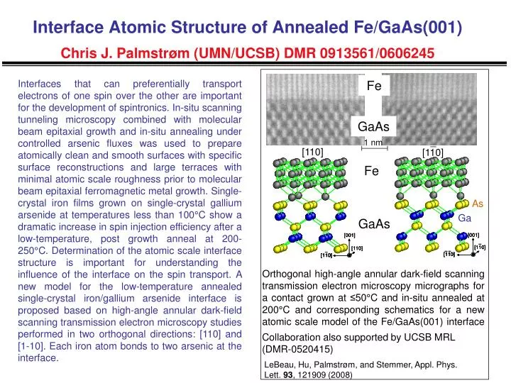
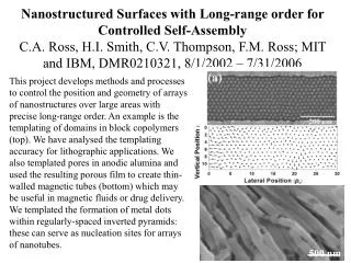
_ [110] Interface Atomic Structure of Annealed Fe/GaAs(001)Chris J. Palmstrøm (UMN/UCSB) DMR 0913561/0606245 Interfaces that can preferentially transport electrons of one spin over the other are important for the development of spintronics. In-situ scanning tunneling microscopy combined with molecular beam epitaxial growth and in-situ annealing under controlled arsenic fluxes was used to prepare atomically clean and smooth surfaces with specific surface reconstructions and large terraces with minimal atomic scale roughness prior to molecular beam epitaxial ferromagnetic metal growth. Single-crystal iron films grown on single-crystal gallium arsenide at temperatures less than 100°C show a dramatic increase in spin injection efficiency after a low-temperature, post growth anneal at 200-250°C. Determination of the atomic scale interface structure is important for understanding the influence of the interface on the spin transport. A new model for the low-temperature annealed single-crystal iron/gallium arsenide interface is proposed based on high-angle annular dark-field scanning transmission electron microscopy studies performed in two orthogonal directions: [110] and [1-10]. Each iron atom bonds to two arsenic at the interface. Fe GaAs 1 nm [110] Fe As Ga GaAs Orthogonal high-angle annular dark-field scanning transmission electron microscopy micrographs for a contact grown at ≤50°C and in-situ annealed at 200°C and corresponding schematics for a new atomic scale model of the Fe/GaAs(001) interface Collaboration also supported by UCSB MRL (DMR-0520415) LeBeau, Hu, Palmstrøm, and Stemmer, Appl. Phys. Lett. 93, 121909 (2008)
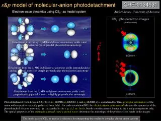
Mentoring of Young Scientistsand Equipment DevelopmentChris J. Palmstrøm (UMN/UCSB) DMR 0913561/0606245 Ms. Shu Lo, a Materials Science undergraduate, developed a compression jig and installed it in a magneto optic Kerr system to measure the magnetostriction in epitaxial Co2MnGe and Fe films grown in the Gen-II EMOF Heusler alloy growth system. A Gen-II EMOF molecular beam epitaxy system was extensively modified by rotating the growth chamber so all sources face upwards. Optical access ports were installed in front of the effusion cells for atomic absorption flux monitoring during growth. In addition, a solid-state detector was incorporated for energy dispersive x-ray spectrometry for composition analysis during growth. Magneto Optic Kerr System with Ms. Shu Lo’s compression system mounted. Completed Heusler alloy growth system


![Nm]](https://cdn3.slideserve.com/6300766/slide1-dt.jpg)