Download
1 / 46
580 likes | 1.64k Views
Asynchronous and Synchronous Counters. Week 10 and Week 11 (Lecture 1 of 2). Counters. * Counters are important digital electronic circuits. * They are Sequential logic circuits because timing is obviously important and they need a memory characteristic.

E N D
Asynchronous and Synchronous Counters Week 10 and Week 11 (Lecture 1 of 2)
Counters • * Counters are important digital electronic circuits. • * They are Sequential logic circuits because timing is obviously important and they need a memory characteristic. • * Digital counters have the following important characteristics, • Maximum number of count • Up-Down Count • Asynchronous or Synchronous Operation • Free-Running or Self-Stopping
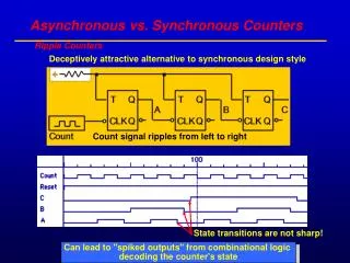
Asynchronous/Ripple Counter • Asynchronous counter are commonly referred to as ripple counter because the effect of the input clock pulse is first “felt” by first flip-flop (FF0). • Cannot get to the second flip-flop (FF1) immediately because of the propagation delay through FF0. • So the effect of an input clock pulse “ripples” through the counter, taking some time, due to propagation delays, to reach the last flip-flop. Only the first FF receive clock pulse from the source ( clock genarator), others FFs receive clock pulse from either Q or Q’ of prior FF
Asynchronous/Ripple Counter Propagation delays in a 3-bit asynchronous (ripple-clocked) binary counter.
Asynchronous/Ripple Counter Three-bit asynchronous binary counter and its timing diagram for one cycle. RIPPLE COUNTER UP – PGT AND ALL NON FIRST CLK RECEIVE CLK PLUSE FROM Q’
Asynchronous/Ripple Counter Four-bit asynchronous binary counter and its timing diagram. RIPPLE COUNTER UP – NGT AND ALL NON FIRST CLK RECEIVE CLK PLUSE FROM Q
Asynchronous Decade Counter • The Modulus of a counter is the number of unique states that the counter will sequence through. • Counter can also be designed to have a number of states in their sequence that is less than the maximum of 2n. • Counters with the states in their sequence are called decade counters. • To obtain a truncated sequence, it is necessary to force the counter to recycle before going through all of its possible states. • One way to make the counter recycle after the count of nine (1001) is to decode count ten (1010) with a NAND gate and connect the output of the NAND gate to the clear (CLR) inputs of the flip-flops. The inputs the NAND gate are from the Q output from FF1 and FF3 ( from 1010 -- FF3FF2FF1FF0)
Asynchronous Decade Counter An asynchronously clocked decade counter with asynchronous recycling. MOD 10 RIPPLE UP COUNTER – NGT AND ALL NON FIRST CLK RECEIVE CLK PLUSE FROM Q MOD 10 AS RESET / CLITCH AT 1010. • The inputs the NAND gate are from the Q output from FF1 and FF3 ( from 1010 -- FF3FF2FF1FF0)
Synchronous binary Counter The term Synchronous refers to events that have a fixed time relationship with each other AND receive cllock pulse from a common source 2-bit synchronous binary counter.
Synchronous binary Counter A 3-bit synchronous binary counter.
Synchronous binary Counter A 4-bit synchronous binary counter and timing diagram. Points where the AND gate outputs are HIGH are indicated by the shaded areas.
Synchronous Counter Design Several methods are available that follow arbitrary sequence. Here we will learn one common method using JK flip-Flops. In synchronous counters all the FF’s are clocked at the same time. J-K Excitation Table Before begin the designing we must know the operation of the J-K FF, let us analysis Truth table for 74LS76 IC (JK flip-flop) and its excitation table.
Synchronous Counter Design J-K Excitation Table 0 0 TRANSITION; FF’s Present status is 0 and it should remain in 0 when a clock pulse is applied. That can be either J=K=0 status or J=0,K=1. That mean J=0 and K=0 or 1 That’s J=0 and K=X(don’t care)
Synchronous Counter Design 0 1 TRANSITION: The present state is 0 and it has to change to 1. This can happen either J=1 and K=0 or J=K=1. That mean always J=1 and K=0 or1 J=1 and K=X( don’t care) 1 0 TRANSITION; The present state is 1 and it has to change to 0. This can happen either J=0 and K=1 or J=K=1. That mean always K=1 and J=0 or1 K=1 and J=X( don’t care) 1 1 TRANSITION; The present state is 1 and it has to change to 1. This can happen either J=K=0 or J=1 and K=0. That mean always K=0 and J can be either level K=0 and J=X( don’t care)
Synchronous Counter Design Design Procedure Given a Counter sequence,
Synchronous Counter Design / Example (1) STEP -1 Draw the state transition diagram showing all the possible states, including those that are not part of the desired counting sequence
Synchronous Counter Design / Example (1) ….cont. STEP -2 Use the state transition diagram to set up a table that lists all PRESENT states and their NEXT states
Synchronous Counter Design / Example (1) ….cont. STEP -3 Add a column to this table for each J and K input. For each PRESENT state, indicate the level required at each J and K input in order to produce the transition to the NEXT state.
A A 1 X X 1 0 X X 1 BC BC 0 X X X 1 X X 1 Synchronous Counter Design / Example (1) ….cont. STEP- 4 Design the logic expression to generate the level required at each J and K, using K-maps. jA= kA= 1
A A X 0 1 X 0 X X 0 BC BC X 1 X 1 X 0 X 1 jB= A Synchronous Counter Design / Example (1) ….cont. STEP- 4 …..cont. kB= A+C
A A X 0 0 X X 1 1 X BC BC X 1 X 1 0 X 1 X Synchronous Counter Design / Example (1) ….cont. STEP- 4 …..cont. kC= 1 jC= AB
Synchronous Counter Design / Example (1) ….cont. SETP -5 Finally to implement the final expressions.
Synchronous Counter Design / Example (2) ? Design a JK synchronous counter that has the following sequence:000,010,101,110 and repeat. The undesired states 001,011,100 and 111 must always go to 000 on the next clock pulse. STEP -1 :State Transition Diagram
Synchronous Counter Design / Example (2) ….cont. STEP- 2 : Table to list PRESENT and NEXT status
Synchronous Counter Design / Example (2) ….cont. STEP- 3 : Table indicate the Level required at each J and K inputs in order to produce the transition to the NEXT
Synchronous Counter Design / Example (2) ….cont. STEP- 4 :Design the logic circuits to generate the levels required at each J and K inputs
Synchronous Counter Design / Example (2) ….cont. STEP- 5 :Simplify the SOP expression using K-maps
Synchronous Counter Design / Example (3) ? Design a JK synchronous counter that has the following sequence:000,010,101,110 and repeat. For undesired states their NEXT states can be DON’T CARES. STEP -1 :State Transition Diagram
Synchronous Counter Design / Example (3) ….cont. STEP- 2 : Table to list PRESENT and NEXT status
Synchronous Counter Design / Example (3) ….cont. STEP- 3 : Table indicate the Level required at each J and K inputs in order to produce the transition to the NEXT
Synchronous Counter Design / Example (3) ….cont. STEP- 4 :Design the logic circuits to generate the levels required at each J and K inputs
Synchronous Counter Design / Example (3) ….cont. STEP- 5 :Simplify the SOP expression using K-maps
Synchronous Counter Design / Example (4) ….cont. Objective: To design a 3 bit counter (D FF) with the following count sequence 7,6,5,4,1. All unwanted stages go to 7. Output sequence 7,6,5,4,1 In 3 bits format: 111,110, 101, 100, 001 State transition diagram: 000 010 111 011 110 101 001 100
Synchronous Counter Design / Example (4) ….cont. Truth table for NGT D flip-flop D Flip Flop Excitation Table:
Synchronous Counter Design / Example (4) ….cont. K- Map Pls draw the cct as a home work
Synchronous Counter Design / Example (5) ….cont. Objective: To design a 3 bit counter (T FF) with the following count sequence 7,6,5,4,1. All unwanted stages go to 7. SOLUTION Output sequence 7,6,5,4,1 In 3 bits format: 111,110, 101, 100, 001 State transition diagram: 000 010 111 011 110 101 001 100
Synchronous Counter Design / Example (5) ….cont. Truth table for NGT T flip-flop
Synchronous Counter Design / Example (5) ….cont. T Flip Flop Excitation Table:
Synchronous Counter Design / Example (5) ….cont. T Flip Flop Input Function Table
Synchronous Counter Design / Example (5) ….cont. K- Map Pls draw the cct as a home work
Synchronous Counter Design / Execise Objective: To design a 3 bit counter (JK FF) with the following count sequence 4,5,7,1,3. All unwanted stages go to 4.