1 / 6

Mechanical drawing for front end chip output pads arrangement

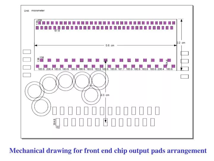
Mechanical drawing for front end chip output pads arrangement. Front end chip. Output pads. Input pad. Front end chip outline, simulation input pads and output pad arrangement. Part of AD620 amplifier for front end chip Vth and Vref. Part of ADG436 switch for

brian-russo
Download Presentation

Mechanical drawing for front end chip output pads arrangement

An Image/Link below is provided (as is) to download presentation Download Policy: Content on the Website is provided to you AS IS for your information and personal use and may not be sold / licensed / shared on other websites without getting consent from its author. Content is provided to you AS IS for your information and personal use only. Download presentation by click this link. While downloading, if for some reason you are not able to download a presentation, the publisher may have deleted the file from their server. During download, if you can't get a presentation, the file might be deleted by the publisher.

E N D

Presentation Transcript


  1. Mechanical drawing for front end chip output pads arrangement

  2. Front end chip Output pads Input pad Front end chip outline, simulation input pads and output pad arrangement

  3. Part of AD620 amplifier for front end chip Vth and Vref Part of ADG436 switch for front end chip calibration signals

  4. Part of FPGA pins which will be tested In Xilinx board

  5. Part of SMB connector for Front end chip calibration signals Part of jumper for front end chipVs

  6. Part for SSD detector outline with two pad for bias

More Related