Download
1 / 71
710 likes | 951 Views
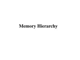
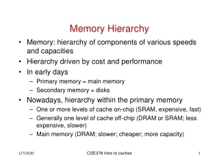
Memory Hierarchy. µProc 60%/yr. 1000. CPU. 100. Processor-Memory Performance Gap: (grows 50% / year). Performance. 10. DRAM 7%/yr. DRAM. 1. 1986. 1987. 1988. 1989. 1990. 1991. 1992. 1993. 1994. 1995. 1996. 1997. 1998. 1980. 1981. 1982. 1983. 1984. 1985. 1999. 2000.

E N D
µProc 60%/yr. 1000 CPU 100 Processor-Memory Performance Gap:(grows 50% / year) Performance 10 DRAM 7%/yr. DRAM 1 1986 1987 1988 1989 1990 1991 1992 1993 1994 1995 1996 1997 1998 1980 1981 1982 1983 1984 1985 1999 2000 Processor-Memory Gap • Memory is an active area of computer architecture. • Due to the expanding gap between advances in processor speed and memory speed.
Technology Trends Capacity Speed (latency) Logic: 2x in 3 years 2x in 3 years DRAM: 4x in 3 years 2x in 10 years Disk: 4x in 3 years 2x in 10 years DRAM Generations Year Size Cycle Time 1980 64 Kb 250 ns 1983 256 Kb 220 ns 1986 1 Mb 190 ns 1989 4 Mb 165 ns 1992 16 Mb 120 ns 1996 64 Mb 110 ns 1998 128 Mb 100 ns 2000 256 Mb 90 ns 2002 512 Mb 80 ns 2006 1024 Mb 60ns 16000:1 4:1 (Capacity) (Latency)
Processor-DRAM Performance Gap Impact: Example • To illustrate the performance impact, assume a single-issue pipelined CPU with CPI = 1 using non-ideal memory. • The minimum cost of a full memory access in terms of number of wasted CPU cycles: CPU CPU Memory Minimum CPU cycles or Year speed cycle Access instructions wasted MHZ ns ns 1986: 8 125 190 190/125 - 1 = 0.5 1989: 33 30 165 165/30 -1 = 4.5 1992: 60 16.6 120 120/16.6 -1 = 6.2 1996: 200 5 110 110/5 -1 = 21 1998: 300 3.33 100 100/3.33 -1 = 29 2000: 1000 1 90 90/1 - 1 = 89 2003: 2000 .5 80 80/.5 - 1 = 159 2006: 3700 0.27 60 60/.27 – 1 = 221
Pentium 4 Cache hierarchy Processor Cycles: 2 L1 I (12Ki) L1 D (8KiB) Cycles: 19 L2 cache (512 KiB) Cycles: 43 L3 cache (2 MiB) Cycles: 206 Memory
Main Memory • Main memory generally uses Dynamic RAM (DRAM), which uses a single transistor to store a bit, but requires a periodic data refresh (~every 8 msec). • Cache uses SRAM: Static Random Access Memory • No refresh (6 transistors/bit vs. 1 transistor/bit for DRAM) • Size: DRAM/SRAM 4-8, Cost & Cycle time: SRAM/DRAM 8-16 • Main memory performance: • Access time: The time it takes between a memory access request and the time the requested information is available to cache/CPU. • Memory bandwidth: The maximum sustained data transfer rate between main memory and cache/CPU.
Conventional DRAM Organization • d x w DRAM: • dw total bits organized as d supercells of size w bits 16 x 8 DRAM chip cols 0 1 2 3 memory controller 0 2 bits / addr 1 rows supercell (2,1) 2 (to CPU) 3 8 bits / data internal row buffer
Reading DRAM Supercell (2,1) • Step 1(a): Row access strobe (RAS) selects row 2. • Step 1(b): Row 2 copied from DRAM array to row buffer. 16 x 8 DRAM chip cols 0 memory controller 1 2 3 RAS = 2 2 / 0 addr 1 rows 2 3 8 / data internal row buffer
To CPU supercell (2,1) supercell (2,1) Reading DRAM Supercell (2,1) • Step 2(a): Column access strobe (CAS) selects column 1. • Step 2(b): Supercell (2,1) copied from buffer to data lines, and eventually back to the CPU. 16 x 8 DRAM chip cols 0 memory controller 1 2 3 CAS = 1 2 / 0 addr 1 rows 2 3 8 / data internal row buffer internal buffer
addr (row = i, col = j) bits 56-63 bits 48-55 bits 40-47 bits 32-39 bits 24-31 bits 16-23 bits 8-15 bits 0-7 63 63 56 56 55 55 48 48 47 47 40 40 39 39 32 32 31 31 24 24 23 23 16 16 15 15 8 8 7 7 0 0 64-bit double word at main memory address A 64-bit doubleword at main memory address A 64-bit doubleword Memory Modules : supercell (i,j) DRAM 0 64 MB memory module consisting of eight 8Mx8 DRAMs DRAM 7 Memory controller
Impact on Performance • Suppose a processor executes at • Clock Rate = 200 MHz (5 ns per cycle) • CPI = 1.1 • 50% arith/logic, 30% ld/st, 20% control • Suppose that 10% of memory operations get 50 cycle miss penalty • CPI = ideal CPI + average stalls per instruction = 1.1(cyc) +( 0.30 (datamops/ins) x 0.10 (miss/datamop) x 50 (cycle/miss) ) = 1.1 cycle + 1.5 cycle = 2. 6 • 58 % of the time the processor is stalled waiting for memory! • a 1% instruction miss rate would add an additional 0.5 cycles to the CPI!
Memory Hierarchy • The idea is to build a memory subsystem that consists of: • Very small, very fast, very expensive memory “close” to the processor. • Larger, slower, but more affordable memory “further away” from the processor. • Hence, provide the appearance of virtually unlimited memory while minimizing delays to the processor. • The memory hierarchy is organized into levels of memory with the smaller, more expensive, and faster memory levels closer to the CPU: registers, then primary Cache Level (L1), then additional secondary cache levels (L2, L3…), then main memory, then mass storage (virtual memory).
Registers Cache Main Memory Magnetic Disc Optical Disk or Magnetic Tape Levels of The Memory Hierarchy Part of The On-chip CPU Datapath 16-256 Registers Farther away from The CPU Lower Cost/Bit Higher Capacity Increased Access Time/Latency Lower Throughput One or more levels (Static RAM): Level 1: On-chip 16-64K Level 2: On or Off-chip 128-512K Level 3: Off-chip 1M-64M DRAM, RDRAM 16M-16G Interface: SCSI, RAID, IDE, 1394 4G-100G
Faster Processor Control Tertiary Storage (Tape) On-Chip Level One Cache L1 Datapath Registers A Typical Memory Hierarchy(With Two Levels of Cache) Larger Capacity Virtual Memory, Secondary Storage (Disk) Second Level Cache (SRAM) L2 Main Memory (DRAM) 10,000,000s (10s ms) 10s Speed (ns): 1s 100s 10,000,000,000s (10s sec) Ks Size (bytes): 100s Ms Gs Ts
Managed by compiler Managed by OS, hardware, application Managed by hardware Memory Hierarchy: Apple iMac G5 Goal: Illusion of large, fast, cheap memory Let programs address a memory space that scales to the disk size, at a speed that is usually as fast as register access
L1 (64K Instruction) Registers 512K L2 (1K) L1 (32K Data) iMac’s PowerPC 970: All caches on-chip
Core0 Core1 L2 Cache Case study: Intel Core2 Duo Source: http://www.sandpile.org
Memory Hierarchy: MotivationThe Principle Of Locality • Programs usually access a relatively small portion of their address space (instructions/data) at any instant of time (loops, data arrays). • Two Types of locality: • Temporal Locality: If an item is referenced, it will tend to be referenced again soon. • Spatial locality: If an item is referenced, items whose addresses are close by will tend to be referenced soon . • The presence of locality in program behavior (e.g., loops, data arrays), makes it possible to satisfy a large percentage of program access needs (both instructions and operands) using memory levels with much less capacity than program address space.
Locality Example • Locality Example: • Data • Reference array elements in succession (stride-1 reference pattern): • Reference sum each iteration: • Instructions • Reference instructions in sequence: • Cycle through loop repeatedly: Spatial locality Temporal locality Spatial locality Temporal locality sum = 0; for (i = 0; i < n; i++) sum += a[i]; return sum;
Memory Hierarchy Operation • If an instruction or operand is required by the CPU, the levels of the memory hierarchy are searched for the item starting with the level closest to the CPU (Level 1 cache): • If the item is found, it’s delivered to the CPU resulting in a cache hit. • If the item is missing from an upper level, resulting in a miss, the level just below is searched. • For systems with several levels of cache, the search continues with cache level 2, 3 etc. • If all levels of cache report a miss then main memory is accessed. • CPU « cache « memory: Managed by hardware. • If the item is not found in main memory resulting in a page fault, then disk (virtual memory), is accessed for the item. • Memory « disk: Managed by hardware and the operating system.
Memory Hierarchy: Terminology • A Block:The smallest unit of information transferred between two levels. • Hit: Item is found in some block in the upper level (example: Block X) • Hit Rate: The fraction of memory access found in the upper level. • Hit Time: Time to access the upper level which consists of RAM access time + Time to determine hit/miss • Miss: Item needs to be retrieved from a block in the lower level (Block Y) • Miss Rate= 1 - (Hit Rate) • Miss Penalty: Time to replace a block in the upper level + Time to deliver the block to the processor • Hit Time << Miss Penalty Lower Level Memory Upper Level Memory From Processor Blk X Blk Y To Processor
Smaller, faster, more expensive device at level k caches a subset of the blocks from level k+1 8 Level k: 9 14 3 Data is copied between levels in block-sized transfer units Caching in a Memory Hierarchy 4 10 10 4 0 1 2 3 Larger, slower, cheaper storage device at level k+1 is partitioned into blocks. 4 4 5 6 7 Level k+1: 8 9 10 10 11 12 13 14 15
General Caching Concepts • Program needs object d, which is stored in some block b. • Cache hit • Program finds b in the cache at level k. E.g., block 14. • Cache miss • b is not at level k, so level k cache must fetch it from level k+1. E.g., block 12. • If level k cache is full, then some current block must be replaced (evicted). Which one is the “victim”? • Placement policy: where can the new block go? E.g., b mod 4 • Replacement policy: which block should be evicted? E.g., LRU Request 12 Request 14 14 12 0 1 2 3 Level k: 14 4* 9 14 3 12 4* Request 12 12 4* 0 1 2 3 Level k+1: 4 5 6 7 4* 8 9 10 11 12 13 14 15 12
Cache Design & Operation Issues • Q1: Where can a block be placed in cache? (Block placement strategy & Cache organization) • Fully Associative, Set Associative, Direct Mapped. • Q2: How is a block found if it is in cache? (Block identification) • Tag/Block. • Q3: Which block should be replaced on a miss? (Block replacement) • Random, LRU. • Q4: What happens on a write? (Cache write policy) • Write through, write back.
Types of Caches: Organization • DM and FA can be thought as special cases of SA • DM 1-way SA • FA All-way SA
Cache Organization & Placement Strategies • Placement strategies or mapping of a main memory data block onto cache block frame addresses divide cache into three organizations: • Direct mapped cache: A block can be placed in one location only, given by: (Block address) MOD (Number of blocks in cache) • Advantage: It is easy to locate blocks in the cache (only one possibility) • Disadvantage: Certain blocks cannot be simultaneously present in the cache (they can only have the same location)
C a c h e 0 1 0 1 0 1 1 0 0 0 1 1 0 0 1 1 0 0 0 0 1 1 1 1 0 1 0 0 1 0 0 0 0 1 0 0 1 0 1 0 1 1 0 1 1 0 0 0 1 1 0 1 0 1 1 1 0 0 1 1 1 1 0 1 M e m o r y Cache Organization: Direct Mapped Cache A block can be placed in one location only, given by: (Block address) MOD (Number of blocks in cache) In this case: (Block address) MOD (8) 8 cache block frames (11101) MOD (1000) = 101 32 memory blocks cacheable
0x0F 00000 00000 0x55 11111 0xAA 0xF0 11111 Direct Mapping Index Tag Data 0 00000 0 0x55 0x0F 1 00000 1 00001 0 • Direct mapping: • A memory value can only be placed at a single corresponding location in the cache 11111 0 0xAA 0xF0 11111 1
Cache Organization & Placement Strategies • Fully associative cache: A block can be placed anywhere in cache. • Advantage: No restriction on the placement of blocks. Any combination of blocks can be simultaneously present in the cache. • Disadvantage: Costly (hardware and time) to search for a block in the cache • Set associative cache: A block can be placed in a restricted set of places, or cache block frames. A set is a group of block frames in the cache. A block is first mapped onto the set and then it can be placed anywhere within the set. The set in this case is chosen by: (Block address) MOD (Number of sets in cache) • If there are n blocks in a set the cache placement is called n-way set-associative. • A good compromise between direct mapped and fully associative caches (most processors use this method).
0x0F 0000 0000 0x55 1111 0xAA 0xF0 1111 Set Associative Mapping (2-Way) Way Way 1 Way 0 Index Data Tag 0 0000 00 0x55 0x0F 1 0000 01 0001 10 • Set-associative mapping: • A memory value can be placed in any of a set of corresponding locations in the cache 1111 10 0xAA 0xF0 1111 11
0x0F 0x0F 0000 0000 0000 0000 0x55 0x55 1111 1111 0xAA 0xAA 0xF0 0xF0 1111 1111 000000 0x55 0x0F 000001 000110 111110 0xAA 0xF0 111111 Fully Associative Mapping Tag Data 000000 0x55 0x0F 000001 000110 • Fully-associative mapping: • A memory value can be anywhere in the cache 111110 0xAA 0xF0 111111
Cache Organization Tradeoff • For a given cache size, we can trade off between hit rate and complexity • If L = number of lines (blocks) in the cache, L = Cache Size / Block Size How many places Name of Number of Setsfor a block to go cache type 1 Direct Mapped L n n-way set associative L/n L Fully Associative 1 Number of comparators needed to compare tags
An Example • Assume a direct mapped cache with 4-word blocks and a total size of 16 words. • Consider the following string of address references given as word addresses: • 1, 4, 8, 5, 20, 17, 19, 56, 9, 11, 4, 43, 5, 6, 9, 17 • Show the hits and misses and final cache contents.
Main memory block no in cache 0
Main memory block no in cache 0 1
Main memory block no in cache 0 1 2
Address 5: Hit, access block 1 of cache Cache Memory Block # Block # 0 0 1 1 0 0 2 2 3 3 4 4 5 5 1 1 6 6 7 7 8 8 9 9 2 2 10 10 11 11 0 12 1 13 3 3 2 14 3 15 16 17 4 18 19 20 21 Main memory block no in cache 0 1 2
Main memory block no in cache 0 5 2
Main memory block no in cache 4 5 2
Main memory block no in cache 4 5 2
Main memory block no in cache 4 5 14
Main memory block no in cache 4 5 2
Main memory block no in cache 4 5 2
Main memory block no in cache 4 1 2
Main memory block no in cache 4 1 10
Main memory block no in cache 4 1 10
Main memory block no in cache 4 1 10