Download
1 / 16
330 likes | 992 Views
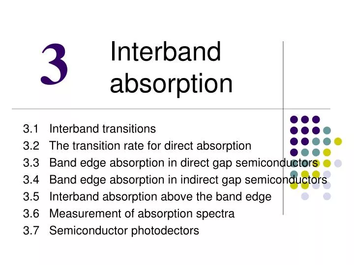
3. Interband absorption. 3.1 Interband transitions 3.2 The transition rate for direct absorption 3.3 Band edge absorption in direct gap semiconductors 3.4 Band edge absorption in indirect gap semiconductors 3.5 Interband absorption above the band edge

E N D
3 Interband absorption 3.1 Interband transitions 3.2 The transition rate for direct absorption 3.3 Band edge absorption in direct gap semiconductors 3.4 Band edge absorption in indirect gap semiconductors 3.5 Interband absorption above the band edge 3.6 Measurement of absorption spectra 3.7 Semiconductor photodectors
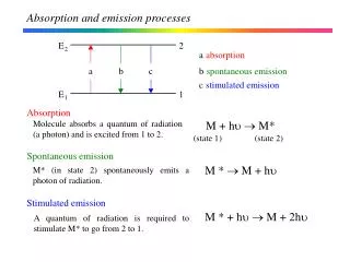
3.1 Interband transition Isolated atom discrete energy level Solid band (delocalized state) For semiconductor or insulator, photon excites electron from filled valence to the empty conduction band, the transtion energy is • There is a continuous range of frequency; • There is a threshold h > Eg= (Ef— Ei)min; • Creation of an electron-hole pair; • Direct and Indirect band gap.
3.1 Interband transition 3.1 Interband transition Absorption and emission of phonon In a direct band material, both the conduction band minimum and the valence band minimum occur at the zone centre where k = 0; In a indirect band gap material, the conduction band minimum does not occur at k = 0, but is usually at the zone edge or close to it. Photon absorption 3.2 The transition rate for direct absorption The optical absorption coefficient Wi -> f transition rate, (Fermi’s golden rule) • Where • the matrix element M, • thedensity of states g(h).
3.2 The transition rate for direct absorption • the joint density of states This gives: • the matrix element M, (semiclassical approach) Perturbation: Dipole moment: Light wave: The electron state wave function: Initial: Final:
3.3 Band edge absorption in direct gap semiconductors 3.3.1 The atomic physics of the interband transitions Electron level in a covalent crystal made from four-valent atom such as Ge or bi- nary compounds such as GaAs. The s And p states of the atoms hybridize to form bonding and antibonding molecular orbitals, which then evolve into the con- duction and valence bands of the semi- conductor 4s24p2 • Selection rules: • The parity of the initial and final states must be different. • j = -1, 0 or +1.(Total angular momentum must change by one unit) • l = 1. • ms = 0. (Spin quantum numbers never change). • Electric-dipole transition: high transition rate, short radiative lifetime(10-9– 10-8 s)–fluorescence. • Magnetic dipole or electric quadrpole: smaller transition rates and longer radiative lifetime • (10-6 s upwards) –the slow emission by electric dipole-forbidden is called – phosphorescence.
3.3 Band edge absorption in direct gap semiconductors 3.3.2 The band structure of a direct gap III-V semiconductor s antibonding p bonding S-like conduction and three p-like valence band Band structure of GaAs. The dispersion of the bands is shown for two directions of the Brillouin zone centre: X and L. The point co- responds to the zone centre with a wave vector of (0,0,0), while the X and L points correspond respectively to the zone edges along the (100) and (111) directions. The valence bands are Below the Fermi level and are full of electrons. (heavy hole band) (light hole band) (split-off hole band)
3.3 Band edge absorption in direct gap semiconductors 3.3.3 The joint density of states 等于能量 时的状态对密度 ) ( Fig.1 The dispersion of band (E— k relationship) The energy conservation of a heavy hole or a light hole transition: Generally,
3.3.4 The frequency dependence of the band edge absorption • Frequency dependence approximately obeyed • The coulomb attraction of excitons neglected; • Impurity or defect states within gap neglected; • The parabolic band approximation only valid • near k = 0. Square of the optical absorption coefficient versus photon energy for the direct gap III-V semiconductor InAs at room temperature. The band gap can be deduced to be 0.35 eV by extrapolating the absorption to zero. 3.3.5 The Franz-Keldysh effect Two main effects on band edge absorption by application of an external electric field E: Electro-optic effect: The electric field modulated optical constants (n,). (K-K relationship). Electroreflectance: The reflectivity can be changed due to modulated optical constants (n,).
3.3.6 Band edge absorption in a magnetic field The electrons in magnetic field: The quantized energy (Landau levels): The transition energy: (cyclotron frequency) The absorption spectrum with kZ=0 given by: The energies electrons and holes within the bands are given by: • Two consequences: • The absorption edge shifts by heBZ/2; • Equally spaced peaks in the spectrum. Quantized motion in the (x, y) plane, free motion in the z direction. E=0 at the top of the valence band: Fig.2 The interband transition creates an electron in the conduction band and a hole in valence band Transmission spectrum of germanium of germanium for B=0 and B=3.6T at 300 K. The electron effective mass can be determined from the energies of minima. Selection rule: n = n’,kZ = k’Z . (the momentum is negligible)
3.4 Band edge absorption in indirect gap semiconductor The indirect transition involve both photons and phonons (h, hq ): Absorption coefficient of indirect band gap: This is a second-order process, the transition rate is much smaller than for direct absorption. • The differences: • Threshold; • Frequency dependence. • The differences provide a way to determine • whether the band gap is direct or not. ( 接下页) As T decrease, phonons decrease gradually. At very low T, no phonons excited with enough energy. Thus at the lowest T, the indirect absorption edge is determined by phonon emission rather than phonon absorption; 5. The direct absorption dominates over the indirect processes once h > 0,8eV, is the band gap for the transition at the Comparison of the absorption coefficient of GaAs and Silicon near their band edges. GaAs has a direct band gap at 1.42 eV, while silicon has an indirect gap at 1.12 eV. The absorption rises much faster with frequency in a direct gap material, and exceeds the indirect material.
3.4 Band edge absorption in indirect gap semiconductor The absorption coefficient of germanium Band structure of germanium. 1. vs h close to the band gap at 0.66 eV ; 2. The straight line extrapolates back to 0.65 eV, which indicates that a phonon(TA)of energy ~ 0.01 eV has been absorbed and q (phonon) = k(electron) atL-point of the Brillouin zone; 3. A tail down to 0.6 eV, this is caused by absor- ption of the higher frequency and also multi- phonons absorption; 4. The temperature dependence of the absorption edge: 1. The lowest conduction band minimum occurs at the L point (k=/a(1,1,1), not at (k=0); 2. Indirect gap=0.66eV, direct gap ()= 0.8eV; Table 3.1 Bose-Einstein Formula (接上页)
Th e interband absorption spectrum of silicon The band structure of silicon 3.5 Interband absorption above the band edge Eg is indirect and occurs at 1.1 eV; E1 and E2 are the separation of the bands at the L and X points, where the conduction and valence are approximately parallel along the (111) and (100). E1 = 3.5 eV is the minimum direct separation, and corresponds to the sharp increase in absorption at E1, and E2 correspond to the absorption maximum at 4.3 eV. Absorption at these energies is very high due to the Van Hove singularities in the joint density of states ( band are parallel. E for direct transition does not depend on k, dE/dk =0, g(E) diverges (critical point) 1. The optical properties at the band edge determine the emission spectra; 2. The spectrum can be worked out by dE/dk fromthe full band structure.
3.6 Measurement of absorption spectra • The measurement of absorption coefficient: • Measure transmission coefficient; • 2. Measure reflectivity spectra R (h) Self-consistent fitting of the reflectivity spectra using the Kramers-Kronig formula.
3.7.1 Photodiodes The fraction of light absorbed in a length l : Photocurrent Ipc : quantum efficiency, the flux of photons per unit time (A/W) If 3.7 Semiconductor photdectors The operating principles: Light with photon energy greater than the band gap is absorbed in the semiconductor, and this create free electrons in the conduction band and free hole in the valence band. The presence of the light can therefore be detected either by measuring a change in resistance of the sample or by measuring an electrical current in an external circuit. The p-i-n photodiode is operated in reverse bias with a positive voltage Vo applied to the n-region. This generates of a strong DC electric field E across the i-region. Absorption of photons in the i-region creates free electron – and hole that are attracted to the n-region and p-regions respectively then flow into the circuit by the field, generating the photocurrent I pc
3.7 Semiconductor photdectors 3.7.2 Photoconductive devices The device relies on the change of the conduc- tivity of material when illuminated by light. The conductivity increase due to the generation of free carriers after absorption of photons by interband transitions. Compared with photodiodes, the detectors are simpler, but tend to have slow response times. 3.7.3 Photovoltaic devices (solar cell) The device generates a photovoltage when irradiated by light. This in turn can be used to generate electrical power in an external power.
Exercises(3): • Indium phosphide is a direct gap III-V semiconductor with a band gap of 1.35 eV at room temperature. The absorption coefficient at 775 nm is 3.5 *106 m-1. A platelet sample 1 m thick is made with antireflection coated surfaces. Estimate the transmission of the sample at 620 nm.(0.37%) • The band parameters of the four-band model shown in Fig.1 are given for GaAs in Table C.2. i) Calculate the k vector of the electron excited from the heavy hole band to the conduction band in GaAs when a photon of energy 1.6 eV is absorbed at 300 K. What is the corresponding value for the light hole transition? ii) calculate the ratio of the joint density of states for the heavy and light hole transitions. What is the wavelength at which transition from the split-off hole band become possible?( i) 5.3*108m-1 and 4.1*108m-1; ii)2.1; iii) 740 nm. • i) Show that the density of state of a particle which is free to move in one dimension only is proportional to E-1/2, where E is the energy of the particle. Ii) Draw a sketch of the frequency dependence of the optical absorption edge of a one-dimensional direct-gap semiconductor. Iii) Explain why a bulk semiconductor in a strong magnetric field can be considered as a one-dimensional system. Hence explain the shape of the optical transmission spectrum of Ge at 300 K at 3.6 T given in Fig. 2 . Iv) Use the data in Fig.2 to deduce values for the band gap and the electron effective mass of Ge on the assumption that mh* >> me* . ( i) (2m/Eh2)-1/2; • ii) ~(h-En)-1/2; iv) 0.035 m0 and 0.8 eV.)