Download
1 / 13
130 likes | 151 Views
This overview covers various design examples in logic building blocks and explores arithmetic circuits, including 2's complement addition and subtraction.

E N D
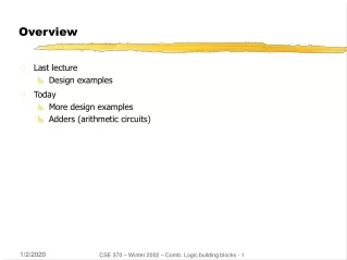
Overview • Last lecture • Design examples • Today • More design examples • Adders (arithmetic circuits) CSE 370 – Winter 2002 – Comb. Logic building blocks - 1
Logical function unit • Multi-purpose function block • 3 control inputs to specify operation to perform on operands • 2 data inputs for operands • 1 output of the same bit-width as operands C0 C1 C2 Function Comments0 0 0 1 always 10 0 1 A + B logical OR0 1 0 (A • B)' logical NAND0 1 1 A xor B logical xor1 0 0 A xnor B logical xnor1 0 1 A • B logical AND1 1 0 (A + B)' logical NOR1 1 1 0 always 0 3 control inputs: C0, C1, C22 data inputs: A, B1 output: F CSE 370 – Winter 2002 – Comb. Logic building blocks - 2
C0 C1 C2 A B F 0 0 0 0 0 1 0 0 0 0 1 1 0 0 0 1 0 1 0 0 0 1 1 1 0 0 1 0 0 0 0 0 1 0 1 1 0 0 1 1 0 1 0 0 1 1 1 1 0 1 0 0 0 1 0 1 0 0 1 1 0 1 0 1 0 1 0 1 0 1 1 0 0 1 1 0 0 0 0 1 1 0 1 1 0 1 1 1 0 1 0 1 1 1 1 0 1 0 0 0 0 1 1 0 0 0 1 0 1 0 0 1 0 0 1 0 0 1 1 1 1 0 1 0 0 0 1 0 1 0 1 0 1 0 1 1 0 0 1 0 1 1 1 1 1 1 0 0 0 1 1 1 0 0 1 0 1 1 0 1 0 0 1 1 0 1 1 0 1 1 1 0 0 0 1 1 1 0 1 0 1 1 1 1 0 0 1 1 1 1 1 0 01234567 AB F AB 8:1 MUX AB S2 S1 S0 C0 C1 C2 Formalize the problem choose implementation technology5-variable K-map to discrete gatesmultiplexer implementation 10 CSE 370 – Winter 2002 – Comb. Logic building blocks - 3
ROM vs. PLA • ROM approach advantageous when • design time is short (no need to minimize output functions) • most input combinations are needed (e.g., code converters) • little sharing of product terms among output functions • ROM problems • size doubles for each additional input • can't exploit don't cares • PLA approach advantageous when • design tools are available for multi-output minimization • there are relatively few unique minterm combinations • many minterms are shared among the output functions • PAL problems • constrained fan-ins on OR plane CSE 370 – Winter 2002 – Comb. Logic building blocks - 4
Regular logic structures for two-level logic • ROM – full AND plane, general OR plane • cheap (high-volume component) • can implement any function of n inputs • medium speed • PAL – programmable AND plane, fixed OR plane • intermediate cost • can implement functions limited by number of terms • high speed (only one programmable plane that is much smaller than ROM's decoder) • PLA – programmable AND and OR planes • most expensive (most complex in design, need more sophisticated tools) • can implement any function up to a product term limit • slow (two programmable planes) CSE 370 – Winter 2002 – Comb. Logic building blocks - 5
Regular logic structures for multi-level logic • Difficult to devise a regular structure for arbitrary connections between a large set of different types of gates • efficiency/speed concerns for such a structure • in 467 you'll learn about field programmable gate arrays (FPGAs) that are just such programmable multi-level structures • programmable multiplexers for wiring • lookup tables for logic functions (programming fills in the table) • multi-purpose cells (utilization is the big issue) • Use multiple levels of PALs/PLAs/ROMs • output intermediate result • make it an input to be used in further logic CSE 370 – Winter 2002 – Comb. Logic building blocks - 6
Combinational logic implementation summary • Multi-level logic • conversion to NAND-NAND and NOR-NOR networks • transition from simple gates to more complex gate building blocks • reduced gate count, fan-ins, potentially faster • more levels, harder to design • Time response in combinational networks • gate delays and timing waveforms • hazards/glitches (what they are and why they happen) • Regular logic • multiplexers/decoders • ROMs • PLAs/PALs • advantages/disadvantages of each CSE 370 – Winter 2002 – Comb. Logic building blocks - 7
Arithmetic circuits • Excellent examples of combinational logic design • Time vs. space trade-offs • doing things fast may require more logic and thus more space • example: carry lookahead logic • Arithmetic and logic units • general-purpose building blocks • critical components of processor datapaths • used within most computer instructions CSE 370 – Winter 2002 – Comb. Logic building blocks - 8
2s complement (fast review) • If N is a positive number, then the negative of N ( its 2s complement or N* ) is N* = 2n – N, where n is the number of bits in the representation • example: 2s complement of 7 • example: 2s complement of –7 • shortcut: 2s complement = bit-wise complement + 1 • 0111 -> 1000 + 1 -> 1001 (representation of -7) • 1001 -> 0110 + 1 -> 0111 (representation of 7) 4 2 = 10000 7 = 0111 1001 = repr. of –7 subtract 4 2 = 10000 –7 = 1001 0111 = repr. of 7 subtract CSE 370 – Winter 2002 – Comb. Logic building blocks - 9
2s complement addition and subtraction • Simple addition and subtraction – 4 + (– 3) – 7 1100 1101 11001 4 + 3 7 0100 0011 0111 4 – 3 1 0100 1101 10001 – 4 + 3 – 1 1100 0011 1111 CSE 370 – Winter 2002 – Comb. Logic building blocks - 10
Why can the carry-out be ignored? • Can't ignore it completely • needed to check for overflow (see next two slides) • When there is no overflow, carry-out may be true but can be ignored – M + N when N > M:M* + N = (2n – M) + N = 2n + (N – M)ignoring carry-out is just like subtracting 2n – M + – N where N + M 2n–1(– M) + (– N) = M* + N* = (2n– M) + (2n– N) = 2n – (M + N) + 2nignoring the carry, it is just the 2s complement representation for – (M + N) CSE 370 – Winter 2002 – Comb. Logic building blocks - 11
–1 +0 –1 +0 +1 +1 –2 –2 0000 0000 1111 1111 1110 1110 0001 0001 –3 –3 +2 +2 1101 0010 1101 0010 –4 –4 +3 +3 1100 0011 1100 0011 –5 –5 1011 1011 0100 0100 +4 +4 1010 1010 0101 0101 –6 –6 +5 +5 1001 1001 0110 0110 1000 0111 +6 1000 0111 +6 –7 –7 +7 +7 –8 –8 Overflow in 2s complement addition/subtraction • Overflow conditions • add two positive numbers to get a negative number • add two negative numbers to get a positive number 5 + 3 = –8 –7 – 2 = +7 CSE 370 – Winter 2002 – Comb. Logic building blocks - 12
Overflow conditions • Overflow when carry into sign bit position is not equal to carry-out 0 1 1 1 0 1 0 10 0 1 1 1 0 0 0 1 0 0 0 1 0 0 1 1 1 1 01 0 1 1 1 5 3 – 8 – 7 – 2 7 overflow overflow 0 0 0 0 0 1 0 1 0 0 1 0 0 1 1 1 1 1 1 1 1 1 0 1 1 0 1 11 1 0 0 0 5 2 7 – 3 – 5 – 8 no overflow no overflow CSE 370 – Winter 2002 – Comb. Logic building blocks - 13