Download
1 / 22
220 likes | 334 Views
From hybrids pixels to smart vertex detectors using 3D technologies. 3D microelectronics technologies for trackers. Outlook. Introduction : Which technologies and what are the challenges ? A process "embedded" 3D : Tezzaron / Chartered example

E N D
From hybrids pixels to smart vertex detectors using 3D technologies 3D microelectronics technologies for trackers
Outlook WIT 2012 Pisa, 3-5 May 2012 • Introduction : Which technologies and what are the challenges ? • A process "embedded" 3D : Tezzaron/ Chartered example • Post-processed 3D : convenient processes for new tracker architectures ? • Conclusions
Which technologies for our challenges ? WIT 2012 Pisa, 3-5 May 2012 • HL LHC : high luminosity, high pile up , high dose • To keep the tracker performance one need to improve pixel granularity: • reduce occupancy • improve resolution ( and 2 tracks separation) • reduce inefficiencies in the readout • Several ways (solutions?) for pixels detectors themselves • move to higher density technology like 65 nm • move to 3D electronics with in-pixel TSVs • move to CMOS HV (see talk I.Peric) • Ways for evolution of global architecture of the trackers • Post-processed 3D New module concepts
"Process embedded " 3D A disappointing experience ? WIT 2012 Pisa, 3-5 May 2012
Goals FE-I4 CMOS 130 nm 50 μm 250 μm FE-TC4 CMOS 130 nm 2 layers 50 μm 125 μm WIT 2012 Pisa, 3-5 May 2012 • Reduce pixel area without changing tech. node by association of 2 or more layers of 3D technologies • Needs in-pixel communication between the 2 tiers small TSVs part of the process itself • Main advantage : Adequate techno selection for the various functions • Main drawback : Few (very few) vendors at the moment
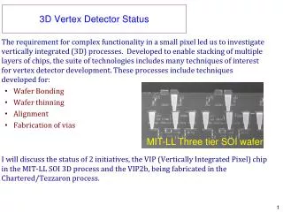
sensor Back SideMetal Super Contact Tier 1 (thinnedwafer) M1 M2 M3 M4 M5 M6 Bond Interface M6 M5 M4 M3 M2 M1 Tier 2 Super Contact Tezzaron-Chartered 3D run Main technology features • 130 nm • Large reticle (≈26 x 30 mm) • 6 metal levels (M6 is the bond interface) • Wafer to wafer, face to face bonding • Vias 1.6 x 1.6 µm with 3.2 µm pitch • Bond interface : copper • Upper tier thinned down to 10 µm Many production problems • Design rules evolution • Chartered-GF restructuration • Tezzaron hybridization tools No complete 3D at the moment but some interesting results WIT 2012 Pisa, 3-5 May 2012 3D consortium created in 2008 (with MAPS and Hybrid pixel communities) and 3D run in 2009
FE-TC4-P1 FE-TC4 analogue part FE-TC4 digital simple part WIT 2012 Pisa, 3-5 May 2012 Pixel matrix of 14 x 61 pixels , pixel size 50 x 166 µm Analog tier is very close to FE-C4-P1 (GF version of FE-I4-P1) Digital tiers in 2 flavors : DC (Bonn design) close to FE-I4 one, DS not intended for read-out but for studying coupling between tiers Only one electrical connection per pixel (discriminator output) Design of each tier allow separate test (even in 3D stack) Analog tier, DC tier, DS tiers tested separately (February 2011) First 3D assemblies AE-DC and AE-DS arrived in (September 2011)
3D wafers WIT 2012 Pisa, 3-5 May 2012 Defects visible to the naked eye
What's happened? WIT 2012 Pisa, 3-5 May 2012 • Bond interface between 2 wafers is done by dense copper bonds • These bonds are mainly mechanical (just few of them have electrical function) • Alignment should be "perfect" to avoid poor mechanical adhesion Problem in thinning top wafer and massive short
Results • After dicing and wire-bond of these few chips • The 2 tiers can be operated separately (tier at the bottom is powered through the top one) • No one chip demonstrates in-pixel communication WIT 2012 Pisa, 3-5 May 2012 • Only few chips on the wafers should be powered • Other ones having massive shorts between power supplies
Analogue part Noise < 100 e- rms WIT 2012 Pisa, 3-5 May 2012 The 10 µm thick analog part behaves as un-thinned one
Complex digital fully working WIT 2012 Pisa, 3-5 May 2012 • "A la FE-I4" read-out • 4 pixel regions • Simplified periphery and control logic • Fully tested at Bonn Fully working even if the floating inputs (due to unconnected analog pixels) produce spurious hits
Shielding studies with Digital Simple 11 “DRUM” cells (noise generator) “DRUM” cell structure: Digital input (test) or Tier1 output Read-out shift register (1b) Test Shielding strategy : • 5 columns without any shielding (reference), • 4 columns with shielding in metal 5, • 2 columns with shielding in metal 3, • 2 columns with both shielding. 13 WIT 2012 Pisa, 3-5 May 2012
S curveswith "Drums" activation Col 6 Row 39 (no shielding) 72e- 240 e- No DRUM WIT 2012 Pisa, 3-5 May 2012 If no shielding Noise increase by a factor 3 ! Shielding with M5 proved to be efficient (no difference with/ without digital activity)
Conclusions for "in-process" 3D WIT 2012 Pisa, 3-5 May 2012 • A "leaning" 3D stack • Many difficulties during the process (3 years !! ) • But : • 2D technology (Chartered/GF) results compatible with IBM ones even for radiation hardness • No performance degradation with thinning (10 µm) • Run replaced for free (we are again waiting for the wafers !) • New runs foreseen this year (through CMP / Mosis)
"Post-processed 3D" New ways to build trackers? WIT 2012 Pisa, 3-5 May 2012
Purposes backside metal lines on FE TSVs pass. comp. flex pass. comp. flex FE-Chip Sensor Sensor FE-Chip WIT 2012 Pisa, 3-5 May 2012 • Look at the 3D post-process capabilities in order to find new ways to build modules and staves • Material reduction (estimation for IBL : 0.13% of X0) • Direct connection of service lines (or flex) on chips bakside
Ongoing efforts WIT 2012 Pisa, 3-5 May 2012 • Various groups working in this direction in ATLAS • Orsay(LAL), Munich, Bonn, CPPM • 2 main Europeans vendors • IZM (Berlin and Munich) • LETI (Grenoble) with 3D initiative
IZM Berlin / Bonn University Cu electroplating – interconnection plug to Al pad Al pad opening by wet etching BEOL SiO2 stack etching Bump deposition and dicing Front side processing Donewith Atlas FE-I2 chip Thin chip! 90µm Back side processing Tapered side walls TSV Backside redistribution metal WIT 2012 Pisa, 3-5 May 2012
FE-I2 modules with TSV Module "backside" Module front side RDL WIT 2012 Pisa, 3-5 May 2012 FE-I2, 90 µm thick with TSV et RDL Hybridized on N-N sensor 2 mounted on board
FE-I2 modules with TSV Noise map, No HV Noise map, HV = -80V connected connected disconnected disconnected Connected pixels: ~180e Disconnected pixels: ~130e WIT 2012 Pisa, 3-5 May 2012 • Chips with TSV are working fine • No extra noise induced by TSV process • But lot of disconnected pixels No handle wafer used • Use FE-I4 chip and the thin flip chip method yet used for FE-I4 • Bonn/CPPM with Aida funding
Conclusions WIT 2012 Pisa, 3-5 May 2012 • 3D microelectronics technologies are rapidly evolving (with the industry needs). • Interesting results for our community are yet obtained • These technologies could certainly offer some "revolution" in tracker world • New modules and stave concepts • Coupling HV-CMOS sensor with RoC by direct copper bonding?