Download
1 / 35
480 likes | 1.17k Views
Chapter 9 Thin film deposition. Introduction to thin film deposition. Introduction to chemical vapor deposition (CVD). Atmospheric Pressure Chemical Vapor Deposition (APCVD). Other types of CVD (LPCVD, PECVD, HDPCVD…). Introduction to evaporation.

E N D
Chapter 9 Thin film deposition • Introduction to thin film deposition. • Introduction to chemical vapor deposition (CVD). • Atmospheric Pressure Chemical Vapor Deposition (APCVD). • Other types of CVD (LPCVD, PECVD, HDPCVD…). • Introduction to evaporation. • Evaporation tools and issues, shadow evaporation. • Introduction to sputtering and DC plasma. • Sputtering yield, step coverage, film morphology. • Sputter deposition: reactive, RF, bias, magnetron, collimated, and ion beam. • Deposition methods for thin films in IC fabrication. • Atomic layer deposition (ALD). • Pulsed laser deposition (PLD). • Epitaxy (CVD or vapor phase epitaxy , molecular beam epitaxy). NE 343: Microfabrication and thin film technology Instructor: Bo Cui, ECE, University of Waterloo; http://ece.uwaterloo.ca/~bcui/ Textbook: Silicon VLSI Technology by Plummer, Deal and Griffin
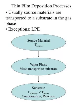
Physical vapor deposition (PVD): evaporation and sputtering In PVD, chemical reactions are not involved, except for reactive (add reactive gases into chamber) evaporation or reactive sputter deposition, which are not widely used. • Evaporation: • Material source is heated to high temperature in vacuum either by thermal or e-beam methods. • Material is vapor transported to target in vacuum. • Film quality is often not as good as sputtered film (that involves energetic bombardment of ions to the as-deposited film, which makes the film denser). • The film thickness can be monitored precisely using a quartz balance – this is necessary as the deposition is not reproducible (tiny change in T leads to large change of deposition rate. T is not monitored, power is). • Sputter deposition: (there is also sputter etching) • Material is removed from target by momentum transfer. • Gas molecules are ionized in a glow discharge (plasma), ions strike target and remove mainly neutral atoms. • Sputtered atoms condense on the substrate. • Not in vacuum, gas (Ar) pressure 5-50mTorr.
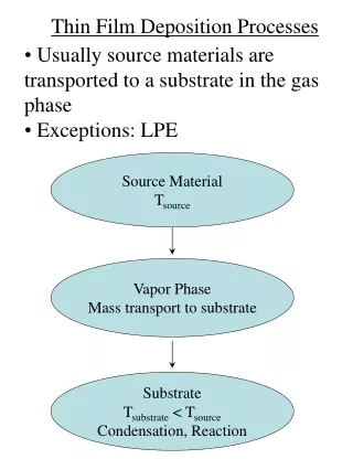
Evaporation (also called vacuum deposition) • In evaporation, source material is heated in high vacuum chamber (P < 10-5Torr), hence the name vacuum deposition. • High vacuum is required to minimize collisions of source atoms with background species (light of site deposition) • Heating is done by resistive or e-beam sources. • Surface interactions are physical, can be very fast (>1m/min possible, but film quality may suffer. For R&D typical 0.1-1nm/sec). • High sticking coefficient (at low T, adatom stays wherever it hits with limited surface migration), leading to poor conformal coverage/significant shadow. But this also makes evaporation the most popular thin film deposition for nanofabrication using liftoff process. • Deposition rate is determined by emitted flux and by geometry of the source and wafer. • Evaporation is not widely used by industry – sputter deposition is. • For microfabrication R&D, evaporation is as important as sputter deposition.
wafer v 2s source Evaporation: vacuum pressure and mean free path Assume a particle of diameter , moving in speed v. Collision cross-section = 2 Collision volume swept during dt = 2 vdt # of collisions during dt = (n/V) 2 vdt Here n/V is number density. Average mean free path = vdt/# = [(n/V) 2]-1 In more rigorous treatment, (PV=nkT) Assume s = 3Å, T= 300K If =30 cm, then a pressure <2.6x10⁻⁴Torris required. Typical vacuum for evaporation <510-6Torr P(Torr) (cm) = 7.8x10⁻³ 1Torr = 1mmHg = 1/760atm
Influence of background vacuum pressure Time to form a single complete layer of gas on a surface, assume sticking coefficient = 1. 1bar=100000Pa (1atm=1.013bar) 1mbar=100Pa 1Torr=100000/760=132Pa=1.32mbar
Arrival ratio Arrival ratio: Ratio of molecular vapor arrival at 1nm/sec deposition rate to molecular impact of residual gas. Arrival ratio = 1 means the number of film molecules hitting the surface per second is the same as the number of gas molecules. For materials that is very reactive with the gas (such as Ti to O2), the film can be very impure when arrival ration 1. In fact, Ti is used as a pump for ultrahigh vacuum (called Ti pump, where Ti vapor is produced to trap gas in vacuum chamber).
Point source and surface source model (a) Point Source (b) Small Surface Area Source F: flux that strikes area A (atoms or grams per cm-2sec). v: deposition rate (nm/sec). N: density of the material (atoms or grams per cm3). Revp: evaporation rate from the source, in atoms or grams per second. : solid angle, =4 if source emits in all directions; =2 if emits only upward.
Deposition rate across a wafer For typical evaporator: h=40cm. Then for a 4” (10cm) wafer, wafer edge l/h=5/40=0.12 c. Non-ideal, more anisotropic emission from a small surface source. (n>1 in cosn distribution) b. Ideal cosine emission from a small planar surface source. (n=1 in cosn distribution) a. Uniform (isotropic emission from a point source). Figure 9-19
Uniformity on a flat surface Consider deposition rate difference between wafer center and edge: Define uniformity : coscos Source-substrate distance requirement: In practice, it is typical to double this number to give some process margin: • Larger r means: • Bigger chamber • Higher capacity vacuum pump • Lower deposition rate • High evaporantwaste. • Typical lab equipment r=40cm
How to achieve uniform deposition • Use spherical wafer holder: • Point source: put source at center of sphere. • Small surface source: put source on inside surface of sphere (compensates for cosn). Location of source which behaves like an ideal point source Location of source which behaves like an ideal small area surface source Figure 9-18 It is shown that Knudsen-cell behavior (i.e. cos emission from a small surface), rather than point source emission or source with cosn n>1, is close to experimental results. Spherical surface with source on its edge: Angle independent, uniform coating! Knudsen-cell
Langmuir-Knudsen theory for Revp Revp: evaporation rate (g/sec) As: source area (cm2) m: gram-molecular mass (g/mol) T: temperature (K) Pe: equilibrium vapor pressure (Torr) To see whether this makes sense or not, consider the “Knudsen-cell” (i.e. a box of gas with pressure Pe emitting from a small opening into vacuum). Assume all gas molecules move only along x, y, z-direction. Then 1/6 moves along +z direction with velocity v. For opening area A, the emitted number of molecules during time t is: 1/6nA(vt), here n is molecular number density. So per unit emitting area, emitting/evaporation rate is: 1/6nv. A more strict derivation gives flux 1/4nv. z Pe The orifice/opening appears as an evaporation source. x
Vapor pressure of common materials Vapor pressure of 1-10mTorr or more is required to achieve reasonable deposition rates of 0.1-1m/min. (? Seems the number doesn’t match using the equations below)
Thermodynamics of equilibrium vapor pressure Liquid volume VL << vapor volume VV By definition: 1 g = 1/µ mol
Evaporation characteristics of materials . From “Materials science of thin films” by Ohring, 2002.
Chapter 9 Thin film deposition • Introduction to thin film deposition. • Introduction to chemical vapor deposition (CVD). • Atmospheric Pressure Chemical Vapor Deposition (APCVD). • Other types of CVD (LPCVD, PECVD, HDPCVD…). • Introduction to evaporation. • Evaporation tools and issues, shadow evaporation. • Introduction to sputtering and DC plasma. • Sputtering yield, step coverage, film morphology. • Sputter deposition: reactive, RF, bias, magnetron, collimated, and ion beam. NE 343: Microfabrication and Thin Film Technology Instructor: Bo Cui, ECE, University of Waterloo, bcui@uwaterloo.ca Textbook: Silicon VLSI Technology by Plummer, Deal, Griffin
Types of evaporation according to heating method Three types: Thermal evaporator – resistive heating, the only choice for evaporation of organic material. Electron beam evaporator – heated by electron beam, most popular, more expensive than thermal evaporator. Inductive heating (must be unpopular – I have never seen one). Inductive heating: Metal element is wound around crucible and RF power is run through coil. RF induces eddy currents in the charge causing it to heat. Eddy current is caused when a conductor is exposed to a changing magnetic field due to relative motion of the field source and conductor; or due to variations of the field with time. These circulating current create induced magnetic fields that oppose the change of the original magnetic field due to Lenz's law, causing repulsive or drag forces between the conductor and the magnet.
Thermal evaporation Widespread use for materials whose vapor pressure can be reasonable at 1600oC or below. Common evaporant materials: Au, Ag, Al, Sn, Cr, Sb, Ge, In, Mg, Ga; CdS, PbS, CdSe, NaCl, KCl, AgCl, MgF2, CaF2, PbCl2.
Photos of Sharon thermal evaporator Inside bell jar Bell jar
Electron beam evaporation Deflection plates are to raster scan the beam across charge surface. • Using a focused electron beam to heat and evaporate metals, electron temperature can be as high as 10,000 K. Electrons are accelerated by DC 10kV, and current 10s-100s of mA. • Suitable for high Tmelt metals like W, Ta, … • Evaporation occurs at a highly localized point near the beam bombardment spot on the source surface , so little contamination from the crucible (not hot, water cooled). Can one do e-beam evaporation of insulating materials like SiO2?
Photos of e-beam evaporator Mechanical shutter: Evaporation rate is set by temperature of source, but this cannot be turned on and off rapidly. Cooling water Shutter Heat conduction of the hearth limits achievable temperature. Power density: 10kV, up to 1.5A, 0.2-1cm2 15-75kW/cm2. Put crucible here
Comparison of thermal and e-beam evaporation • Thermal evaporation: • Simple, robust, and in widespread use. • Use W, Ta, or Mo filaments to heat evaporation source. • Typical filament currents are 200-300 Amperes. • Exposes substrates to visible and IR radiation. • Contamination from heated boat/crucible. • Electron beam evaporation: • More complex, but extremely versatile, virtually any material. • Less contamination, less heating to wafer (as only small source area heated to very high T). • Exposes substrates to secondary electron radiation. • X-rays can also be generated by high voltage electron beam. • Since x-rays will damage substrate and dielectrics (leads to trapped charge), e-beam evaporators cannot be used in MOSFET.
Popular heating “containers” for evaporation source Resistors (put source rod inside coil) Heating boat (open top) Crucibles (only choice for e-beam evaporator) Box with small opening (Knudsen cell!)
Typical boat/crucible material Considerations: thermal conductivity, thermal expansion, electrical conductivity, wetting and reactivity. Graphite crucible is most popular, but avoid cracking the crucible due to stress/ temperature gradients (bad for materials that “wet” graphite such as Al and Ni). Aluminum: tungsten dissolves in aluminum, so not quite compatible.
How to monitor film thickness during evaporation? 6MHz Quartz Electrode Deposited film Vapor • Quartz Crystal Micro-balance (QCM): (similar idea to quartz clock) • Quartz is a piezoelectric material. • With a high frequency AC voltage activation, the amplitude of vibration is maximum at resonance frequency. • This resonance frequency will shift when film is deposited on its surface. • Thus by measuring frequency shift f, one can measure film thickness with sub-Å accuracy. http://en.wikipedia.org/wiki/Quartz_crystal_microbalance
Evaporation issues: step coverage Step coverage is poor (line of sight and sticking coefficient Sc≈ 1). Heating can decrease Sc, but may change film properties (structure – large grain). Therefore, due to poor step coverage (and x-ray damage), rarely used in IC fabrication. Sticking coefficient: SC = 1 SC < 1 The depositing species have a high Sc so that they are deposited where they first strike. The depositing species have a low Sc, so that many are re-emitted and re-deposited (or migrated) elsewhere on the topography, such as on the sidewalls.
Evaporation issues: alloy evaporation • Stoichiometrical problem of evaporation: • Compound material breaks down at high temperature. • Each component has different vapor pressure, therefore different deposition rate, resulting in a film with different stoichiometry compared to the source. • One solution is co-evaporation (use two e-beam guns).
Shadow evaporation Poor step coverage could be useful. Shadow/angle evaporation is routinely used for nano-electronics fabrication. The pictures above show shadow-masks for niobium rings containing a Josephson junction, prior to evaporation. The metals are evaporated under different angles without breaking the vacuum. The mask consists of Germanium while the sacrificial layer below the mask is made of high temperature capable plastic (polyether sulphone).
GLAD (glancing angle deposition): self assembly of film Angle >80o, with (or without) substrate rotation. Self assembly mainly due to shadowing effect that magnifies the otherwise grain structures. Invented by Michael Brett from University of Alberta http://www.ece.ualberta.ca/~glad/lab.html
Glancing angle deposition (GLAD) Staionary substrate (i.e. no rotation), one evaporation source, Cr films.
Glancing angle deposition (GLAD) Stationary substrate, two evaporation sources, SiO2 films. Independent control of column angle and film porosity. The porosity is constant, the column angle β is controlled between the inclined and vertical angles.
Evaporation: a quick summary • Evaporation advantages: • Films can be deposited at high rates (e.g., 1μm/min, though for research typically < 0.1μm/min). • Low energy atoms (~0.1 eV) leave little surface damage. • Little residual gas and impurity incorporation due to high vacuum conditions. • No or very little substrate heating. • Limitations: • Accurately controlled alloy compounds are difficult to achieve. • No in-situ substrate cleaning. • Poor step coverage (but this is good for liftoff). • Variation of deposit thickness for large/multiple substrates – has to rely on quartz crystal micro-balance for thickness monitoring. • X-ray damage.