Download
1 / 28
280 likes | 429 Views
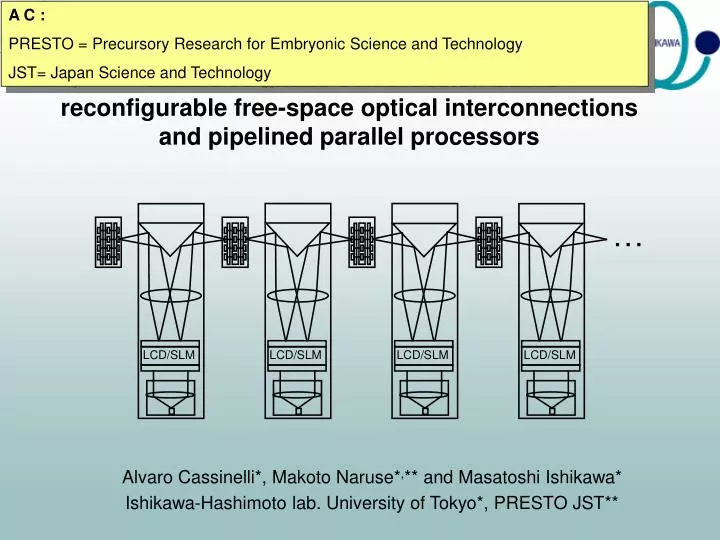
…. LCD/SLM. LCD/SLM. LCD/SLM. LCD/SLM. A C : PRESTO = Precursory Research for Embryonic Science and Technology JST= Japan Science and Technology. Quad-tree image compression using reconfigurable free-space optical interconnections and pipelined parallel processors.

E N D
… LCD/SLM LCD/SLM LCD/SLM LCD/SLM A C : PRESTO = Precursory Research for Embryonic Science and Technology JST= Japan Science and Technology Quad-tree image compression using reconfigurable free-space optical interconnections and pipelined parallel processors Alvaro Cassinelli*, Makoto Naruse*,** and Masatoshi Ishikawa* Ishikawa-Hashimoto lab. University of Tokyo*, PRESTO JST**
Plan of the presentation I. OCULAR architectures for computing - Reconfigurable Single Stage (OCULAR-I) - Reconfigurable Multi-stage (OCULAR-II) II. OCULAR-II demonstration: Quad-tree compression. - Quad-tree compression algorithm - Set-up and Demonstration - Discussion III. Conclusion and further work
O ptoelectronic C omputer U sing L aser A rrays with R econfiguration Processing Element Array VCSEL array Optical Interconnections Photo Detector Array Optical Interconnections 2D array of data … 2D array of data Output VCSEL Processing Element Array Photo Detector Optical feed-back I. OCULAR architectures for computing I.1 Reconfigurable Single Stage (OCULAR-I) I.2 Reconfigurable Multi-stage (OCULAR-II)
I.1 Single-stage paradigm for parallel computing Pn P1 controller Z Y P1 X … … P2 control P2 X … Y … ULA mux … … … Mem … Z … Pn … Optical technology offers enhanced parallel communication primitives network-based parallel computers …of great benefit for = distributed memory shared memory Dynamic Static Reconfigurableinterconnection (X, YorZ). Fixed interconnection (X, Y, andZ) …switches outside processors (local or global/external control possible) …switches inside processors (local control)
I.1 Dynamic architecture vs. static [slide not shown in main presentation] switches interconnections processors Pn P1 P1 … … P2 … … … … … P2 … … Pn … Feed-back loop Technologically challenging Non reusable architecture Bad scalability In an n-degree static topology, each processor has n distinct optoelectronic I/O ports… …anyway, static networks can be redesigned as single-stage dynamic networks… Optimal use of electronic, optoelectronic and optics Scalability, hardware reusability in other topologies possible introduction of multiple stages… …processors, switches and interconnections located in distinct modules
I.1 OCULAR-I system architecture dynamic single stage… …optical architecture Elementary Processor Array P1 X Photo-detector array … … VCSEL array P2 … … Y … … … Optical interconnection module … Z … Pn … Optical feed-back [ Modular architecture ] Switches and interconnections : reconfigurable diffractive optics module 2D optoelectronic processing layer (PD-PE-VCSEL) +
Processing Module [VCSEL array ] [ Photo-detector array ] 850 nm VCSELs Modulation > 1 GHz (possible 10-50 GHz) Si photo-detectors with Integrated amplifier / threshold [ SIMD Processor array ] registers 8x8 PEs (on FPGA) A B local memory (24 bits) ALU mapped I/O PE PD VCSEL Each array attached to a PCB 4-neighbors Electronic mesh for rapid short range communication between PEs. 10 MHz operation demonstrated
Reconfigurable interconnection module X Y Z alvaro: In these optical interconnection module, we require adjustable components to adopt the diffraction position on LD and PD. We have designed zooming Fourier transform lens as the adjustable component. The focal length is adjustable from 360mm to 440mm by moving one of lenses as illustrated in the figure. This function is important for matching interconnection parameters such as the pixel pitches of the VCSEL-array, the PD-array, the CGH, and for compensating for wavelength variation of the VCSEL array. Folded 4-f system The module generates the interconnection pattern… 14 x 25 x 6.2 cm = FT lens Laser diode …it is therefore responsible for interconnection and switching CGH is generated by an optically addressable SLM, using a laser diode and a liquid crystal display coupled trough a fiber optical plate. Space-invariant interconnections – good/bad? Free-space – alignment issues? Multi-level CGH – gooddiffraction efficiency Reconfiguration (“switch”) freq. – 100 Hz…
I.2 Multi-stage paradigm for parallel computing P1 P2 Interconnection … Switch & Pn Benes Clos Delta Cube Cycle Hypercube [computing & networking] Tree [computing] Omega Mesh De Bruijn Banyan Pyramid Shuffle/exchange Single-Stage Multi-Stages architecture can be “spanned” into Stage 1 Stage 2 Stage m P1 P1 P1 P2 P2 P2 S & I - m S & I - 1 S & I - 2 … … … … Pn Pn Pn Simplicity &Speed – S & I does not need to be complex (shuffle-exchange networks). Scalability / Reconfigurability – for different topologies. Pipelining – possible. Theoretical background – Multi-stage architectures have been studied for decades in networking applications… The cost of multiplying the processors is paid back as…
I.2 OCULAR-II system architecture … Optical interconnection module Optical interconnection module Optical interconnection module Optoelectronic processing module Elementary Processor Array Photo-detector array VCSEL array Two layer module
Sender array Electrical feed-back trough host computer PE array VCSELs Interconnection module (SLM) Receiver array Photo Detectors PE array II. Quad-tree compression on OCULAR-II II.1 Quad-tree compression algorithm II.2 Set-up and Demonstration II.3 Discussion
II.1 Principle of the quad-tree compression algorithm Image… …corresponding tree This group of pixels is a level 2 leaf of address B level 3 A B A D C B level 2 B D …this pixel is NOT a leaf B level 1 DB C D A level 0 …this pixel is a level 0 leaf of address CDA level 1 leaf of address DB CDA Leaf = ( level , address ) Image as a tree = ( 2 , B ) + ( 1 , DB ) + ( 0 , CDA )
II.1 Quad-tree compression on OCULAR-II architecture array n+1 array n+2 cutting branches A C : Rem : data from the receiver side to the sender side is electronically feed-back trough the host computer… Load 2Nx2N image.ON pixels are set as lowest level leafs on local PE memories. array n+1 • initialization array n • from stage to stage 2 4 1 • detect upper leaves 3 - sequentially broadcast leaf’s values to corresponding upper PE. - compareon receiver side detect upper leaves - updateleaf levels of upper-level PE, if corners resulted to be lower “false” leafs. • cutting branches - parallel broadcast signal for resetting false low-level leaves. • End on last stage: - Download data from last array. - Save data (level, address) from PEswhich are still leaves.
Example : interconnection for processing of level 1 A B (zero order) (first order) D C D = broadcasting PE on array n = computing PE on array n+1 A B A D C 1) Detecting leaves CCD image of PD plane …Is A a level one leaf? 2) Conditional broadcast …If so, A must update its leaf level and cut lower branches. [slide not shown in main presentation]
II.2 OCULAR-II demonstrator setup • demonstration is carried out on a two layer OCULAR II prototype PE array 1 PE array 2 PD array VCSEL array Multiple layer processing is simulated thanks to electronic feed-back between first and second processor arrays. Optical interconnection module • Interconnection for each level are timemultiplexed on the SLM module. Level 0 Level 2 Level 1 cgh diffraction pattern • Two level CGHs are used (enough diffraction efficiency)
…quad-tree algorithm and hypercube network Y X Z W 2n elementary processors arranged in a n-dimensional hypercube topology Image 2n/2x 2n/2pixel large Quad-tree on OCULAR-II: pairs of (6-dimensional) hypercube links are generated and multiplexed in time thanks to the SLM-based interconnection module… …on level 1: X, Z …on level 2: Y, W …
II.2 Quad-Tree Compression Demonstration Setup CGH monitor “receiver” array (SIMD + PD) Monitor CCD Interconnection module “sender” array (SIMD + VCELS) Control and results on host computer …
Example : holograms required during level 1 processing. B A C D = broadcasting PE = computing PE B A D C 1) Broadcast hologram (quadrant comparison) (first order) (zero order) Potential leaf on level one D 2) Re-Broadcast hologram (cutting branches) A [slide not shown in main presentation]
Level 0.Detecting upper leaves. C D Level 0quadrants A B D C B A true false level 0 leaves …symbolic representation of the initial tree, containing 28 level 0 (most of them false) leaves
Detail of level 0 broadcasting [slide not shown in main presentation] sender array photo-detector chip surface as seen through the alignment CCD camera = “D” corners with leaf bit ON = “D” corners with leaf bit OFF. receiver array In this demonstration we used two-level phase CGHs computed by SA. Only the 1storder of diffraction is used as the interconnection pattern.
Level 0. Cutting branches. D C newly created leaf on level 1 B A
Level 1.Detecting upper leaves. D C Level 1quadrants A B B A D C
Level 1. Cutting branches. D C B A newly created leaf on level 2
Level 2.Detecting leaves and cutting branches. C D Level 2 quadrants B A B A D C …symbolic representation of the encoded image as a minimal tree with seven leaves.
II.3 Discussion Compression of a 2Nx2N pixel large image takesO(5.N) clock cycles... SIMD array, VCSEL and photo-detectors can run at more than 100MHz… two million 1024x1024 images compressed per second! 8x8 image (N=3) 15 iterations… …only seven final leaves 28 pixels ON = 28 initial leaves. However,SLM reconfiguration limits operation at maximum hundred hertz.... Also, one have to remember than our chips are only 8x8 pixel large.
III. Conclusion and further work II.1 Summary II.2 Research underway and further work
I.1 Summary We have successfully tested OCULAR-II multistage architecture with reconfigurable optical interconnections by implementing quad-tree compression on binary images (=example of embedded hypercube) However… Optically addressed SLM-based interconnection module accounts for the strongest bandwidth limitation (hundred hertz) Electronic feed-back trough host computer generates parasitic signals, and synchronization problems! Alignment is not difficult, but may become a critical issue in “true” multistage architectures...
III.2 Further work: OCULAR-III network interconnection modules Processor arrays IBnC [ Research underway ] Alignment issues (between 2D arrays) Fiber bundle - dynamic alignment using actuators and control theory. - pre-aligned connectors using fiber-bundles. Concurrent multistage paradigm using fixed interconnections - design of fixed, guide-wave-based pre-aligned interconnection modules (the processor array is in charge of the switching function) => OCULAR-III Design of an integrated (VLSI) optoelectronic layer (with switching…) [ Future research directions ] - Test of these “modular” architectures for building computing and networking MINs. - Design of all-optical networks using the above paradigm. http://www.k2.t.u-tokyo.ac.jp/index-e.html