Download
1 / 18
180 likes | 293 Views
Trapping-related negative feedback as the reason for collected charge restriction in heavily irradiated Si detectors operating with avalanche multiplication. E. Verbitskaya , V. Eremin , A. Zabrodskii Ioffe Physical-Technical Institute of Russian Academy of Sciences

E N D
Trapping-related negative feedback as the reason for collected charge restriction in heavily irradiated Si detectors operating with avalanche multiplication E. Verbitskaya, V. Eremin, A. Zabrodskii Ioffe Physical-Technical Institute of Russian Academy of Sciences St. Petersburg, Russia Z. Li Brookhaven National Laboratory Upton, NY, USA P. Luukka Helsinki Institute of Physics, Helsinki, Finland 23 RD50 Collaboration Workshop CERN, Geneva, Nov 13-15, 2013
Outline • Motivation • PTI modelof Qc enhancement in irradiated Si detectors • Restriction on collected charge arisen from negative feedback in irradiated Si detectors: comparison with “Quasi-APD” • Stabilization of E(x) in irradiated Si n-on-p strip detectors • Gain in Qcin detectors with various thickness • Comparison with experimental data • Conclusions E. Verbitskaya,, et al., 23 RD50 workshop, Nov 13-15, 2013, CERN
Motivation Experimental results of RD50 Our calculation Detector design: n-on-p, strip Qcmax/Qmip 1.5 – 1.9 - as in the experiments Relatively low! strip n-on-p Qcmax/Qmip1.5 – 1.8; pad (Epi p-on-n) 6-9 (e-h near the surface) Spaghetti diodes Avalanche PhotoDiodes (APD) High electric field + impact ionization - E – hundreds kV/cm, internal gain ~200 (Hamamatzu) and even more What is the origin of restriction on Qcgain in heavily irradiated Si n-on-p strip detectors? Almost no difference in charge collection efficiency for different implants • Extended fluence range • up to 1017neq/cm2 (2013) • stable operation E. Verbitskaya,, et al., 23 RD50 workshop, Nov 13-15, 2013, CERN
Origin of Qc restriction: comparison with imaginary “APD” Hamamatsu APD Irradiated detector is compared with imaginary structure - “Quasi-APD”: n-on-p strip diode E(x) as in heavily irradiated detector (high V) carrier avalanche multiplication but no injection and trapping of holes ttr = 1 ms (no trapping of nonequilibrium carriers) Read structures I ~ 20 pA ( 1.5 mm) E – hundreds kV/cm Internal gain G = Qam/Qo Qc enhancement: Kenh = Qcmax/Qmip In n-on-p strip detectors Kenh= 1.5-1.9 - our calculation and experiment Qo - signal induced on the strip, calculated without avalanche multiplication Qam - signal measured or calculated in the same detector with avalanche multiplication E. Verbitskaya,,et al., 23 RD50 workshop, Nov 13-15, 2013, CERN
Goal Finding the origin of restriction on the collected charge enhancement (gain in collected charge) in heavily irradiated Si n-on-p strip detectors by simulation E(x) and Qcand comparison with Quasi-APD - structure different from classic APD and LGAD Results are published in: E. Verbitskaya, et al., NIM A 730 (2013) 66 E. Verbitskaya,, et al., 23 RD50 workshop, Nov 13-15, 2013, CERN
PTI model of Qcenhancement due to avalanche multiplication in heavily irradiated n-on-p Si strip detectors The PTI model considers: formation of Double Peak (DP) electric field profile – DP E(x); focusing of the electric field and current near the collecting n+ strips; avalanche hole generation near the n+ strips, hole injection into the detector bulk, and hole trapping to radiation-induced deep levels defects give rise to the negative feedbackwhich stabilizes the avalanche multiplication and total detector performance V. Eremin, et al., 14 and 15 RD50 workshops, 2009, Freiburg and Geneva V. Eremin, E. Verbitskaya, A. Zabrodskii, Z. Li, J. Härkönen, NIM A 658 (2011) 145 E. Verbitskaya, V. Eremin, A.Zabrodskii,2012, J. Instrum., v.7, 2, ArtNo: C02061; doi: 10.1088/1748-0221/7/02/C02061 E. Verbitskaya, et al., NIM A 730 (2013) 66 E. Verbitskaya,, et al., 23 RD50 workshop, Nov 13-15, 2013, CERN
PTI model of Qcenhancement via avalanche multiplication and negative feedback E. Verbitskaya,, et al., 23 RD50 workshop, Nov 13-15, 2013, CERN
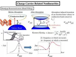
E(x) changes via trapping-related negative feedback Negative feedback in n-on-p detectors: impact ionization near n+ (e, h) hole injection hole trapping to DLs E(x) Emax reduction of –Neff reduction of dE/dx and Emax at n+ reduction of ae,h n+ p+ Trapping-related negative feedback: stabilizes avalanche multiplication and total detector performance BUT simultaneously restricts Qc enhancement Trapping-related or Space Charge Limited Current negative feedback E. Verbitskaya,, et al., 23 RD50 workshop, Nov 13-15, 2013, CERN
Algorithm of E(x) and Qc simulation • Processes considered: • formation of a steady-state E(x)distribution: • equilibrium carriers (bulk generation current) and avalanche generated carriers near • n+ strips, their trapping on radiation-induced DL defects; • charge collection in the detector bulk with a calculated E(x)profile; • e and h are generated by MIPs Procedure and main parameters ♦ Poisson equation combined with the rate equation ♦ one-dimensional approach for detector geometry ♦ Effective deep levels: DA Ec – 0.53 eV; DD Ev + 0.48 eV ♦ 1/te,h=be,hFeq; be= 3.2x10⁻¹⁶cm2ns-1, bh= 3.5x10⁻¹⁶cm2ns-1 ♦ ionization rates ae,h = Ae,hexp(-Be,h/E) (Aand Bfrom B. J. Baliga, ModernPowerDevices, Hoboken, NJ; Wiley, 1987) ♦ numerical calculation E. Verbitskaya,, et al., 23 RD50 workshop, Nov 13-15, 2013, CERN
Simulation of Qc enhancement Variable parameters ♦ detector bias voltage V, ♦ temperature Tin the LHC range, ♦ irradiation fluenceF, ♦ strip detector geometry (strip width, detector thickness) Starting point for simulation – fit to the curve [*] with maximal Qc: F = 3x10¹⁵neq/cm2, T = -20C • * I. Mandić, et al., NIM A 612 (2010) 474) • ** G. Casse, Recent developments in silicon detectors, 13th VCI, Feb 11-15, 2013 Vienna; http:// vci.hephy.at E. Verbitskaya,, et al., 23 RD50 workshop, Nov 13-15, 2013, CERN
Options for E(x) and Qc simulations Kaval – avalanche multiplication Kinj - injection of avalanche generated holes mj - current generation rate Allows differentiation between impact of different factors - E(x) profile, current generation rate, trapping E. Verbitskaya,, et al., 23 RD50 workshop, Nov 13-15, 2013, CERN
Comparative results on E(x), Qc and G Gain at 1800 V n-on-p strip detector; d = 300 mm; pitch/strip width 80/20 (mm) F = 3x10¹⁵neq/cm2 E. Verbitskaya,, et al., 23 RD50 workshop, Nov 13-15, 2013, CERN
E(x) stabilization at different V and F due to negative feedback Stabilization of Emax at n+ strips F= 3x10¹⁵neq/cm2 At F>1x1015 cm-2Emax is insensitive to V • DP E(x) in avalanche multiplication mode • Emaxat n+ strip is stable • Emax stability reduces sensitivity of Qc to the design of the region with high E(shown in the experiments e.g. with spaghetti diodes). At F>5x1015 cm-2 the difference in Emaxin 300 mm and 100 mm detectors is not essential at fixed V E. Verbitskaya,, et al., 23 RD50 workshop, Nov 13-15, 2013, CERN
Qc(F) dependence in n-on-p strip detectors 253K Qc enhancement starts at ~500 V - DP E(x) (d = 300 mm) Qc(F) is nonmonotonous and shows a bump Qc in bump is larger than Qmip Kenh = Qcmax/Qmip =1.4 - 300 mm 1.9 - 100 mm - agrees with experiment E. Verbitskaya, et al.,,2012, J. Instrum., v.7, 2 # C02061 E. Verbitskaya,, et al., 23 RD50 workshop, Nov 13-15, 2013, CERN
Gain in strip detectors with various thickness Similar G in 300 mm and 100 mm detectors at highest V Maximum G is shifted to higher F in 100 mm detectors E. Verbitskaya,, et al., 23 RD50 workshop, Nov 13-15, 2013, CERN
Comparison with experimental results Calculated Qc(F) with a bump correlates to the experiment for thin detectors E. Verbitskaya,, et al., 23 RD50 workshop, Nov 13-15, 2013, CERN G. Casse,20th RD50 Workshop, Bari, 31/05-02/06 2012
Conclusions • Internal gain in collected charge due to avalanche multiplication is strongly suppressed and simultaneously stabilized by the trapping-related negative feedback which is a specific of detectors with high concentration of deep levels. • The gain is in the range 1-6 for both standard and thin detectors, which defines the limit for the signal enhancement and operational fluence range. • Trapping-related negative feedback makes the gain practically insensitive to the design of the detector high field region E. Verbitskaya,, et al., 23 RD50 workshop, Nov 13-15, 2013, CERN
Acknowledgments • This work was made within the framework of CERN RD50 collaboration • and supported in part by: • Fundamental Program of Russian Academy of Sciences on collaboration with CERN, • Russian Federation President Grant # SS-3008.2012.2, • US Department of Energy, contract no DE-AC02-98CH10886 Thank you for attention! E. Verbitskaya,, et al., 23 RD50 workshop, Nov 13-15, 2013, CERN