Download
1 / 18
200 likes | 521 Views
Fundamental reliability issues of advanced charge-trapping memory devices. Luca Larcher and Andrea Padovani Università di Modena e Reggio Emilia, Italy IU.NET, Italy. Non-volatile memory scenario.

E N D
Fundamentalreliabilityissuesofadvancedcharge-trappingmemorydevicesFundamentalreliabilityissuesofadvancedcharge-trappingmemorydevices Luca Larcher and Andrea Padovani Università di Modena e Reggio Emilia, Italy IU.NET, Italy
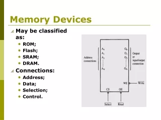
Non-volatile memory scenario • Floating Gate (FG) NAND is the mainstream technology for mass storage applications (multimedia, smart phone, SSD) • Charge Trapping (CT) memories attractive to overcome FG device scaling limits (ITRS 2009) L. Breuil et al., IMW 2010
CT memories: advantages & drawbacks Advantages • Charge stored into discrete traps • better reliability: less sensitivity to defects/SILC • no drain turn on • no erratic/fast erase bits • Bottom SiO2 thickness can be scaled down • better electrostatic and lower operating voltages • Better aspect ratio reduced coupling between adjacent cells • Suitable for 3D architectures (stacked, BiCS, GAA, VG, TCAT, GAA) Drawbacks • Retention at medium-high temperature • Erase saturation (SONOS) • Tradeoff between P/E performances and reliability
Purposes of this talk • Understanding the fundamental reliability issues of planar CT memories, mostly related to high-k materials SiO2, Al2O3, high-k multi-layers (SiO2/Al2O3, HfAlO, LAAlO, ..) gate blockingdielectric SiN (BG engineered), HfO2, HfAlO, Yb2O3, … storagelayer tunnel dielectric SiO2, ONO, high-k VARIOT BGE barrier source drain
Outline • Discrete storage concepts • Band-Gap Engineered (BGE) tunnel dielectrics • VARIOT concepts • High-k blocking dielectrics • Defects assisted charge loss current • Charge trapping into Al2O3 traps
Outline • Discrete storage concepts • Band-Gap Engineered (BGE) tunnel dielectrics • VARIOT concepts • High-k blocking dielectrics • Defects assisted charge loss current • Charge trapping into Al2O3 traps
Horizontal charge localization issues • Charge localization into discrete traps: not uniform along horizontal/vertical directions • Charge displacement induced by charge gradient and self-induced field leads to VT shift in retention and read disturbs • Lateral movement (Poole-Frankel) of separated e-/h+ distribution found in NROM NROM A. Shappir et al., IEEE T-DMR, vol. 4, 2004 - A. Janai et al., IEEE T-DMR, vol. 4, 2004 - A. Furnemount et al., IEEE T-ED, vol. 54, 2007 - C. Kangi et al., IEEE IRPS Proc., 2007
Vertical charge localization issue • e-/h+ distribution in the TANOS SiN after P and E operations forms a vertical dipole • e-/h+charge migration induced explains the opposite polarity of VT shift in retention P+E and E+P (a concern for the memory retention) P+E P+E E+P E+P TANOS L. Vandelli et al., IEEE-IRPS Proc. 2010
Outline • Discrete storage concepts • Band-Gap Engineered (BGE) tunnel dielectrics • VARIOT concepts • High-k blocking dielectrics • Defects assisted charge loss current • Charge trapping into Al2O3 traps
BGE tunnel dielectric: VARIOT • BGE tunnel dielectric allows improving P/E performances without penalizing the reliability • VARIOT is the most promising solution • symmetrical SiO2/high-k/SiO2 stacks • barriers modulated by the electric field • thin/low barrier for fast P/E • thick/high barrier in retention to suppress charge loss H.-T. Lue et al., IEEE-IEDM 2006 - K. K. Likharev,APL, vol.73, 1998 - B. Govoreanuet al., IEEE EDL, vol24, 2003
BGE tunnel dielectric: BE-SONOS • Strong sensitivity of the gate current due to lower field and lower barrier in high-k • Tunnel BGE stacks with several high-k (HfO2, Si3N4, Al2O3, ZrO2, …) demonstrated in CT memory devices: BE-SONOS H.-T. Lue et al., IEDM Tech. Dig., 2005
BGE tunnel dielectric: BE-SONOS -2 • BE-SONOS reliability improved compared to SONOS • negligible cycling effects and charge loss at 85C • Defects in BGE high-k could be a reliability issues • higher TAT leakage current: its effect reduced by the strong immunity to local defects of CT devices • charge trapping reduced by using thin high-k layers and defect passivation (its effect not unambiguously explained) Storagelayers 1 2 source drain H.-T. Lue, IRPS Proc. , 2006 - H.-T. Lue, IRPS Proc., 2009– S. Verma et al. IMW 2009
Outline • Discrete storage concepts • Band-Gap Engineered (BGE) tunnel dielectrics • VARIOT concepts • High-k blocking dielectrics • Defects assisted charge loss current • Charge trapping into Al2O3 traps
TANOS: Al2O3blockingoxide Al2O3 blocking oxide and TaN/TiN metal gate suppress e- current from the gate, improvement of P/E speed and E saturation TANOS reliability issues related to Al2O3 TAT charge loss current through Al2O3 charge trapping into Al2O3 defects TaN Al2O3 SiN SiO2 C.-H. Lee et al., IEDM Tech. Dig., 2003
TAT charge loss through Al2O3 • Charge loss through Al2O3at high VT thanks the lower band-gap of Al2O3 compared to SiO2 • different charge loss rate observed in SONOS and SANOS • Charge loss due to TAT through Al2O3 defect increases VT degradation in read disturbs and data retention Retention in program state M. Chan et al., Microelectronics engineering, vol. 86, 2009 - G. Molas et al., IEDM 2010
Al2O3chargetrappingeffect in TANOS • Electron trapping into Al2O3 accounts for up to 25% of the total VT, depending on SiN/Al2O3 thicknesses (tN/tAL) ratio • Fast DVFB decrease in retention (region I) attributed to electron emission from Al2O3 traps: VT instability and data retention degradation L. Larcher et al., VLSI-TSA Proc., 2010
BGE blocking dielectric • To improve retention without penalty in P/E performances • SiO2 layer insertion improves retention and read disturb because • SiO2 at SiN/Al2O3 interface reduces electron trapping into Al2O3 defects and related reliability issues • Reduction of Al2O3 field diminishes exponentially the TAT current H. Park et al., IMW 2010
Conclusions High-k materials needed to improve NVM reliability and performance lead to VT shifts and instability Feasible solutions for optimum CT-NVM devices: Planar devices with BGE tunnel, blocking and storage layer– very difficult to compete with FG 3D SONOS (BiCS, GAA, VG, ..) – looks promising D. Gilmeret al., IEDM 2009