Download
1 / 23
240 likes | 348 Views
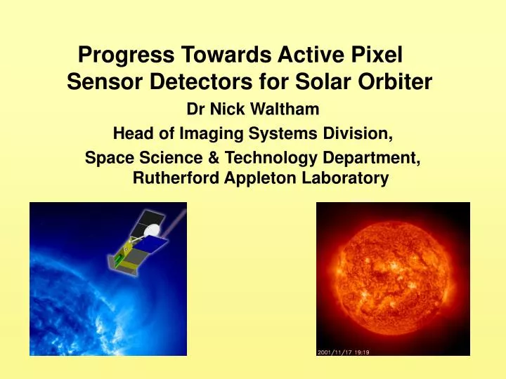
Progress Towards Active Pixel Sensor Detectors for Solar Orbiter Dr Nick Waltham Head of Imaging Systems Division, Space Science & Technology Department, Rutherford Appleton Laboratory. STEREO CCD. Solar Mass Ejection Imager (SMEI). CCDs for Solar Physics. CCDs for Solar Physics

E N D
Progress Towards Active Pixel Sensor Detectors for Solar Orbiter Dr Nick Waltham Head of Imaging Systems Division, Space Science & Technology Department, Rutherford Appleton Laboratory
STEREO CCD Solar Mass Ejection Imager (SMEI) CCDs for Solar Physics . . . CCDs for Solar Physics • e.g. SOHO, SMEI, SOLAR-B, STEREO . . . • Future missions e.g. SDO But inherent limitations . . . • External drive electronics needed. • Solar physics community always want more pixels, more channels, faster readout. • But with smaller/lower size, mass, and power ! And for Solar Orbiter . . . • Radiation damage ! • Protons, neutrons, etc • Loss of charge transfer efficiency ! • Pixel Size ? • Smaller pixels yield a smaller instrument.
CCD ASICs Active Pixels RAL - Current programme . . . SMEI (Solar Mass Ejection Imager) CCD camera • Birmingham University, UCSD, AFRL, • Primary requirement - high dynamic range. • Await launch STEREO/SECCHI solar science mission • CCD camera design for 4 instruments with NRL and Birmingham. • Key requirements - high speed readout, high dynamic range, yet reduced size, mass, and power. • Now feeds into camera designs for SDO AO proposals. R&D Activities • ASIC based CCD camera readout electronics. • CMOS Active Pixel Sensors. Solar Mass Ejection Imager (SMEI)
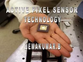
What are we doing about it ? Development of Science-grade CMOS Active Pixel Sensors ! An alternative sensor technology to CCDs . . .
Image sensor with pixels. • Wavelength coverage same as a CCD. • Difference charge sensed inside pixel . • Advantages . . . • CMOS allows on-chip readout circuitry. • Low mass, low power cameras. • Smaller pixel size. Shorter optics / smaller instrument. • Charge sensed inside pixel . . . No charge transfer. Greater radiation tolerance. • What are we doing about it . . . • Science-Grade APS development Program. Pixel Vdd Reset Voltage Reset Source Follower Photodiodes Row Select Column Select What is an Active Pixel Sensor (APS) ?
RAL APS Development Programme 1999 • Design / modelling of pixel test structures (0.5 and 0.7 m CMOS). 2000 • Fabrication and testing of pixel test structures. • Established formal collaboration with Marconi (EEV) • Exchange of designs / ideas, packaging, testing, • Back-thinning Unique capability ! • Design of 512 x 512 pixel sensor (0.5 m CMOS) 2001 • Fabrication of 512 x 512 pixel prototype sensors. • Birmingham join collaboration (Helen Mapson-Menard, Chris Eyles). • EEV thinning test structures and 512 x 512 prototypes. • First tests of 512 x 512 prototypes. • Planning for Solar Orbiter (move to 0.25 m CMOS). 2002 • Design / fabrication of 0.25 m CMOS 4kx3k 5m pixel APS. • Full testing of front and back-illuminated 512 x 512 prototypes.
Pixel Design Test Structure chip with four 16 x 16 pixel arrays • Test Results • QE ~35% 10um active thickness • Noise estimate < 50 electrons rms • Calculated node capacitance = 18 fF • Overall responsivity = 6 V per electron • Peak output signal = 1 volt (167k electrons) • Dark signal = 140 mV per second (0.6 nA/cm2) • Fixed pattern noise = 10mV pk-pk Quadradot Pixel Quantum Efficiency Helen Mapson-Menard Chris Eyles (Birmingham) RAL APS test structure development
512 x 512 Pixel Prototype Pixel Active Pixel Sensor Individual 512 x 512 pixel APS chip 6 inch wafer of 512 x 512 sensors Wire-bonded to an evaluation PCB
512 x 512 Pixel Prototype Pixel Active Pixel Sensor Two test Images
512 x 512 Pixel Prototype Pixel Active Pixel Sensor Note Dynamic range and Anti-blooming Performance ! • So where next ?
ESA’s Solar Orbiter Driven by the proposal of a Spectrometer on Solar Orbiter Detector Requirements • EUV sensitive • Large format (4k x 4k pixels) • Small (5 m pixels) • Science-grade linearity, low-noise, good uniformity • Radiation hard • Low power
Foveon's 16.8-million-pixel APS Solar Orbiter Detector Detector Goals • 4k x 4k pixel sensor • 5m pixel size • 14 bit dynamic range • EUV Sensitive • 4-transistor CDS pixel • 0.25 m rad-hard CMOS process It can be done ! Development Programme • Refine requirement specification • Develop CAD models and simulations • Define architectural design • Design, fabricate, and test 5m pixel test structures • Transfer 14-15 bit ADC to 0.25 m CMOS • Investigate back-thinning with Marconi Demonstrate feasibility in time for the AO !
Standard APS pixel SO 4T pixel Source Follower Input MOS RST RST Reset Switch TX SEL SEL Column Select Switch Transfer Gate Column Output Column Output Ibias Ibias kTC and Fixed-Pattern noise reduction possible by differential readout of dark and signal level. Simplest architecture. No kTC or Fixed-Pattern noise reduction. Solar Orbiter Detector - Photodiode pixels.
Solar Orbiter Detector - Photodiode pixels. Schematic Layout • 4-MOS transistor pixel. • PMOS transfer gate for kTC / FPN noise reduction and increased dynamic range.
DIFFERENTIAL ANALOGUE OUTPUT A 4K x 3K PIXEL ARRAY MULTIPLEXER SAMPLING CAPACITORS DIFFERENTIAL AMPLIFIER PIXEL SELECTION LOGIC Solar Orbiter Detector - Chip Architecture
2 Electron sensor Linear sensor 4,000 pixels at 3 mm pitch 3 1 Area sensor 4,000 * 3,000 = 12 Million pixels 5 mm pitch Solar Orbiter Detector - Progress IC design / manufacturing sharing reduction of costs • Area sensor: ESA’s Solar Orbiter for EUV imaging of Sun 4Kx3K, noise ~ 10 e- rms, DR ~ 12+ bits • Linear sensor: TOPSAT-2 • BNSC Earth Observation 1 m ground resolution, colour, on-chip 10-bit ADCs, ~ 1500 fps • 3.Electron sensor: HEP Vertex (Linear Collider, RHIC upgrade, biomed) intelligence in the pixel, fast readout (50MHz/row), low noise (~ 10 e- rms), data sparsification, radiation resistance 0.25 m CMOS manufactured by TSMC
Solar Orbiter Detector - Progress • 4k x 3k Sensor – Predictions from CAD simulation work • Full Well Capacity ~ 46k electrons (5 m pixel) • Readout Noise ~ 10 electrons rms • Dynamic Range ~ 12+ bits • Fill Factor ~ 30% (but be careful !) • Readout rate ~ 1 MHz (through one port only) • Readout time ~ 12 seconds (full-frame, no windowing)
Solar Orbiter Detector - Future • Future Possibilities • Chips of any format up to 4k x 4k (5 m) pixels. e.g. • 4k x 512 (5 m) pixel strips on selected bands. • 2k x 2k (10 m) pixels. • or you could have odd-shaped pixels (10 x 20 m). • CMOS allows you to design what you want ! • Multi-port readout for higher frame rate. • Windowed readout. • Anything else wanted – besides EUV sensitivity ?
Two different approaches to enhance the EUV sensitivity of silicon APS. • Backthinning ( back-illumination): with Marconi Applied Technology • Front etching of the oxide by Focused Ion Beam EUV sensitivity – Backthinning, or FIB, or ?
EUV Photon < 5m Charge diffusion to adjacent pixels In field-free region EUV Photon Front vs Rear illumination
Solar Orbiter Detector - Future Development Programme • 4k x 3k pixel Array Manufacture (Delivery Dec 02). • Array Packaging (Jan 03). • First light (Feb 03). • Testing of 512 x 512 pixel prototypes (front and rear illuminated). E2V are delivering thinned sensors this week. • Transfer of 14-15 bit ADC to 0.25 m CMOS in second phase. • Thinning of 4k x 3k pixel array and EUV testing.
Summary Requirement EUV Sensitivity 4k x 4k pixels 5 m pixel size Readout < 1 second Low power Cooling Radiation hardness Availability • Science-grade CCD • Yes • Yes (for SDO ?) • No • Not easily • No • -80°C • Poor (CTE degradation) • Soon (12 m pixels) • ? (5 m pixels) APS Probably Yes Yes Yes / Windowed readout Yes -80°C Good (no CTE involved) (2003 – 2006) ?
Solar Orbiter Detector - Alternatives Have considered naked CMOS APS so far. Are there alternatives ? • Diamond / Bold ? Progress towards a large format array ? Smallest pixel ? / Bump bonding ? • CID Radiation hard but limited availability, small range of formats, large pixels, very high read noise. • Intensified APS – like in CDS ?