Download
1 / 29
290 likes | 468 Views
Progress of SOI Pixel Detectors. Sep. 9, 2010 @PIXEL2010 Yasuo Arai, KEK yasuo.arai@kek.jp http://rd.kek.jp/project/soi/. OUTLINE. Overview of SOIPIX activities On-Going R&Ds Buried P-Well Wafer Thinning FZ-SOI Wafer Nested BNW/BPW Structure Double SOI Wafer Summary.

E N D
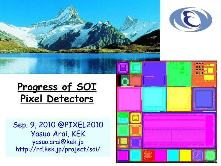
Progress of SOI Pixel Detectors Sep. 9, 2010 @PIXEL2010 Yasuo Arai, KEK yasuo.arai@kek.jp http://rd.kek.jp/project/soi/
OUTLINE Overview of SOIPIX activities On-Going R&DsBuried P-WellWafer ThinningFZ-SOI WaferNested BNW/BPW StructureDouble SOI Wafer Summary • Other SOI related talks • XFEL – MVIA T. Hatusi • ILC Pair Monitor Y. Sato • LBNL/Padva P. Giubilato • Vertical Integration M. Motoyoshi R. Yarema
SOI Pixel Detector Monolithic detector using Bonded wafer (SOI : Silicon-on-Insulator) of Hi-R and Low-R Si layers. • No mechanical bump bondings-> High Density, Low materialbudget-> Low parasitic Capacitance, High Sensitivity • Standard CMOS circuits can be built • Thin active Si layer (~40 nm)-> No Latch Up, Small SEE Cross section. • Based on Industrial standard technology • Seamless connection to Vertical Integration 3
OKI 0.2 mm FD-SOI Pixel Process An example of a SOI Pixel cross section
MPW (Multi Project Wafer) run ~Twice per Year
SOI MPW run Users KEK, Tsukuba Univ., Tohoku Univ., Kyoto Univ., Kyoto U. of Education, Osaka Univ., JAXA/ISAS, RIKEN, AIST LBNL, FNAL, Univ. of Hawaii INP Krakow, INFN Padova, Louvain-la-Neuve Univ., Universität Heidelberg IHEP ChinaBudker Institute of Nucl. Phys. Open to anybody! Supporting Companies OKI Semiconductor Co. Ltd. ,OKI Semiconductor Miyagi Co. Ltd. , T-Micro Co. Ltd., Rigaku Co. Ltd.
KEK SOI Pixels INTPIX4: Integration Type 10.2 mm x 15.4 mm 17x17 mm2, 512x832 (~430k)pixels、13 Analog Out、CDS. CNTPIX5: Counting Type 5 mm x 15.4 mm 64 x 64 mm2, 72 x 272 pixels Amp+Shaper+2xDiscri+2x9b Counter 7 7
Other SOI Pixels Riken - MVIA Kyoto Univ. - XRPIX Fermilab - MAMBO LBNL-AChip
Recent Process Improvements • Increase No. of Metal Layer : 4 -> 5 layers --> Better Power Grid and Higher Integration • Shrink MIM capacitor size : 1 -> 1.5 fF/um2 --> Smaller Pixel size become possible
Recent Process Improvements • Relax drawing rule : 30o, 45o -> Circle --> Smooth field and Higher Break Down Voltage • Introduction of source-inserted body contacts --> Better body contacts (Less kink and history effects, Lower noise).
On-Going R&Ds Back Gate Effect : Sensor voltage affect Transistor characteristics Buried P-Well (BPW) layer Wafer Thinning : Thin Sensor TAICO process Wafer Resistivity : Lower depletion voltage FZ SOI wafer Cross Talk : Reduce coupling between Sensor and Circuit Nested BNW/BPW Structure Radiation Hardness : Compensate traped charge Double SOI Wafer
a. Back Gate Effect Front Gate and Back Gate are coupled. (Back Gate Effect) Vg_back
Buried p-Well (BPW) BPW Implantation Substrate Implantation Buried Oxide (BOX) SOI Si Pixel Peripheral P+ BPW • Cut Top Si and BOX • High Dose • Keep Top Si not affected • Low Dose • Suppress the back gate effect. • Shrink pixel size without loosing sensitive area. • Increase break down voltage with low dose region. • Less electric field in the BOX which may improve radiation hardness.
Id-Vg and BPW w/o BPW with BPW=0V NMOS back channel open shift Back gate effect is suppressed by the BPW.
b. Wafer Thinning :TAIKO process Back side process still can be done after thinning.
Thinned to 110 umand diced I-V Characteristic Before & After Thinning No difference seen after thinning
Infrared Laser (1064 nm) Response of Thinned Chip Full Depleted around 100V
c. Wafer Resistivity : FZ SOI Wafer During the conventional SOI process, many slips were generated in the 8’’ FZ-SOI wafer. Slips We optimized the process parameters, and succeeded to perform the process without creating many slips.
FZ-SOI Wafer Depletion Full Depleted @22V
d. Nested BNW/BPW Structure implant • Signal is collected with the deep Buried P-well. • Back gate and Cross Talk are shielded with the Buried N-well. • Test chip is under process. Structure developed in cooperation between G. Deptuch (Fermilab) and I. Kurachi (OKISemi)
e. Double SOI Layer wafer Increase radiation hardness by compensating Oxide/Interface Trap charge with middle layer bias. circuit additional conduction layer sensor Shield sensors from circuit
Total Ionization Dose effect can be compensated by back bias Leak Current and VTh resumes to nearly original value by biasing back side even after 100Mrad. Vback= 0-10-20-30V 1015 p/cm2 (~100 Mrad) 1015 p/cm2 (~100 Mrad) beforeirradiation
Summary • Our SOI MPW run is operated regularly twice per year. • In addition to many chip designs, a lot of activities are going. • a. Buried P-Well technology is very successful to suppress the Back Gate problem. • b. Thinning to 110um by TAICO process works very well. • c. Wafer resistivity is greatly increased by using FZ-SOI wafer. • d. Nested BNW/BPW structure may resolve cross talk problem and opened possibility of new sensor structure. • e. Manufacturing of Double SOI wafer is being discussed with supply and processing companies. • Vertical integration Motoyoshi san’s Talk
KEK-OKI semi SOI Brief History '05. 7: Start Collaboration with OKI Semiconductor. '05.10: First Submission in VDEC 0.15 um MPW. '06.12: 1st (and last) 0.15 um KEK MPW run. '07.3: 0.15 um lab. process line was closed. --> move to 0.2 um mass production line. '08.1: 1st KEK SOI-MPW run. '09.2: 2nd KEK SOI-MPW run. '09.8: 3rd KEK SOI-MPW run. '10.1: 4th KEK SOI-MPW run. '10.8: 5th KEK SOI-MPW run.
SOI Pixel Process Flow SOI (40 nm) Box (Buried Oxide)(200 nm) 650um Handle Wafer n+ p+ Handle Wafer p+ n+ 50~650um Handle Wafer Al
Integration Type Pixel (INTPIX) b線 Size : 14 mm x 14 mm with CDS circuit 27
Counting Type Pixel (CNTPIX5) 9bit x 8 Time Resolved Imaging Energy selection and Counting in each pixel 5 x15.4 mm2 72 x 272 pixels 64um x 64 um pixel
Integration Type Pixel (INTPIX4) Largest Chip so far. 15 mm 10 mm 17x17 mm, 512x832 (~430k)pixels、13 Analog Out、CDS circuit in each pixel. 29