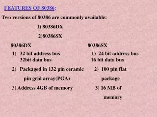
Download
1 / 76
760 likes | 924 Views
80386DX. Programming Model. The basic programming model consists of the following aspects: Registers Instruction Set Addressing Modes Data Types Memory Organization Interrupts and Exceptions. Programming Model. The basic programming model consists of the following aspects: Registers

E N D
Programming Model • The basic programming model consists of the following aspects: • Registers • Instruction Set • Addressing Modes • Data Types • Memory Organization • Interrupts and Exceptions
Programming Model • The basic programming model consists of the following aspects: • Registers • Instruction Set • Addressing Modes • Data Types • Memory Organization • Interrupts and Exceptions
Register Overview • The Intel386 DX has 32 register resources in the following categories: • General Purpose Registers • Segment Registers • Instruction Pointer and Flags • Control Registers • System Address Registers • Debug Registers • Test Registers
General Purpose Registers • hold data or address values. • support data of 1, 8, 16, 32 and 64 bits. • 32-bit registers : EAX, EBX, ECX, EDX, ESI, EDI, EBP, and ESP. • The least significant 16 bits of the registers can be accessed as in 8086 with names of the registers AX, BX, CX, DX, SI, DI, BP, and SP.
General Purpose Registers • When accessed as a 16-bit operand, the upper 16 bits of the register are neither used nor changed. • 8-bit operations can be performed with AL, BL, CL and DL. • The higher bytes are AH, BH, CH and DH • The individual byte accessibility offers flexibility for data operations.
Segment Registers • The segment registers • CS indicates the current code segment • SS indicates the current stack segment • DS, ES, FS and GS indicate four current data segments. • On any data reference the DS-pointed data segment is assumed by default. • In order to access any other data segment, an override directive is used
Instruction Pointer • It is a 32-bit register named EIP. • EIP holds the offset of the next instruction to be executed. • The offset is always relative to the base of the code segment (CS). • The lower 16 bits of EIP contain the 16-bit instruction pointer named IP, which is used by 16-bit addressing.
Bit 17 (VM Bit, Virtual Mode): • VM bit is set to work in Virtual 8086 mode • Bit 16 (RF Bit, Resume Flag): • RF flag is used with debug register breakpoints. • When RF is set, debug fault need to be ignored on the next instruction. • RF is then automatically reset after every instruction
Flag Register • Bit 15 : Reserved • Bit 14 (NT Bit, Nested Task): • This flag applies to Protected Mode. • NT is set to indicate that the execution of this task is nested within another task. • If set, it indicates that the current nested task's Task State Segment (TSS) has a valid back link to the previous task's TSS.
Bit 13,12 (IOPL Bit, Input/output Privilege): • maximum CPL(current privilege level) value permitted to executeI/O instructions without generating anexception 13 fault or consulting the I/O PermissionBitmap.
Bit 11 (OF Bit, Overflow Flag): • OF is set if the operation resulted in a signed overflow. • Bit 10 (DF Bit, Direction Flag): • DF defines whether ESI/EDI registerspost-decrement or post-increment during thestring instructions. • Post-increment occurs ifDF is reset. • Post-decrement occurs if DF isset.
Flag Register • Bit 9 (IF Bit, Interrupt Enable Flag): • When IF =1 the processor allows recognition of external interrupts on INTR pin • Bit 8 (TF Bit, Trap Enable Flag): • When TF =1 the processor enables the single step mode for debugging. • Bit 7 (SF Bit, Sign Flag): • SF is set if the high-order bit of the result isset, it is reset otherwise.
Flag Register • Bit 6 (ZF bit, Zero Flag): • ZF is set if all bits of the result are 0. • Bit 4 (AF Bit, Auxiliary Carry Flag): • The Auxiliary Flag is used to simplify the additionand subtraction of packed BCD numbers. • AF is set if the operation resulted in acarry out of bit 3 (addition) or a borrow into bit3 (subtraction). Otherwise AF is reset. • AF is only for bit 3.
Flag Register • Bit 2 (PF Bit, Parity Flag): • PF is set for even parity. • Bit 0 (CF Bit, Carry Flag): • CF is set for 8-, 16- or 32-bit operations if it results in a carry out of (addition), or a borrow into (subtraction) the high-order bit.
Control Registers • Intel386 DX has 3 control registers(CR0, CR2 and CR3) of 32 bits to hold machine state of a global nature • These registers along with System Address Registers hold machine state that affects all tasks in the system • To access Control Registers, load and store instructions are defined
CR0 : Machine Control Register • CR0 contains 6 defined bits for control and status purposes. • The low-order 16 bits of CR0 is defined as Machine Status Word • To operate only on the low-order 16-bits of CR0, LMSW and SMSW instructions are used. • For 32-bit operations the system should use MOV CR0, Reg instruction.
CR0 : Machine Control Register • Bit 31 (PG Bit, Paging Enable) : The PG bit is set to enable the on-chip pagingunit. • Bit 4 (Reserved) : This bit is reserved by Intel.
CR0 : Machine Control Register • Bit 3 (TS Bit, Task Switched) : TS is automatically set whenever a task switchoperation is performed. • Bit 2 (EM Bit, Emulate Coprocessor) : • Bit 1 (MP Bit, Monitor Coprocessor) :
CR0 : Machine Control Register • Bit 0 (PE Bit, Protection Enable) : • PE =1, enable the Protected Mode. • If PE =0, processor operates in Real Mode.
CR1 : Reserved • CR1 is reserved for use in future Intel processors
CR2 : Page Fault Linear Address • CR2 holds the 32-bit linear address that caused the last page fault detected.
CR3 : Page Directory Base Address • CR3 contains the physical base address of the page directory table. • The Intel386 DX page directory table is always page-aligned (4 Kbyte-aligned). • Thus the lowest twelve bits of CR3 are ignored. • A task switch through a TSS invalidates all page table entries in paging unit cache.
System Address Registers • Four special registers are defined to reference the tables. • These tables or segments are: • GDT (Global Descriptor Table) • IDT (Interrupt Descriptor Table) • LDT (Local Descriptor Table) • TSS (Task State Segment)
System Address Registers • The addresses of these tables and segments are stored in special registers, the System Address and System Segment Registers. • These registers are named GDTR, IDTR, LDTR and TR, respectively
GDTR and IDTR • These registers hold: • 32-bit linear base address and • 16-bit limit • of GDT and IDT respectively. • GDT and IDT segments are global to all tasks in the system.
LDTR and TR • These registers hold 16-bit selector for • LDT descriptor and • TSS descriptor • Since they are task specific, they are defined by selector values stored in system segment registers.
LDTR and TR • A system descriptor register, which is not visible to programmer, is associated with each system segment register
Debug Registers • Debugging of 80386 allows data access breakpoints as well as code execution breakpoints. • 80386 contains 6 debug registers to specify • 4 breakpoints • Breakpoint Control options • Breakpoint Status
Linear Breakpoint Address Registers • Breakpoint addresses are 32-bit linear addresses • While debugging, Intel 386 h/w continuously compares the linear breakpoint addresses in DR0-DR3 with the linear addresses generated by executing software.
Debug Control Register • LENi(i=0 - 3): Breakpoint Length Specification Bits: • 2 bit field for each breakpoint • Specifies length of breakpoint fields • The choices of data breakpoints are 1byte, 2bytes & 4bytes • For instruction execution breakpoint, the length is 1(beginning byte address)
Debug Control Register • RWi(i=0 - 3): Memory Access Qualifier Bit • 2 bit field for each breakpoint • Specifies the type of usage which must occur to activate the associated breakpoint
Debug Control Register • GD: Global Debug Register Access Detect • Debug registers can only be accessed in real mode or at privilege level 0 in protected mode • GD bit, when set, provides extra protection against any Debug Register access even in Real Mode or at privilege level 0 in Protected Mode.
Debug Control Register • GE and LE bit: Exact data breakpoint match, global and local • If either GE or LE is set, any data breakpoint trap will be reported exactly after completion of the instruction that caused the operand transfer. • LE bit is cleared during task switch and is used for task-local breakpoints. • GE bit is unaffected during a task switch and remain enabled during all tasks executing in the system.
Debug Control Register • Gi and Li(i=0 - 3): Breakpoint Enable, global and local • If either Gi and Li is set then the associated breakpoint is enabled.
Debug Status Register • A Debug Status Register allows the exception 1 handler to easily determine why it was invoked. • It can be invoked as a result of one of several events: 1) DR0 Breakpoint fault/trap. 2) DR1 Breakpoint fault/trap. 3) DR2 Breakpoint fault/trap. 4) DR3 Breakpoint fault/trap. 5) Single-step (TF) trap. 6) Task switch trap. 7) Fault due to attempted debug register access when GD = 1.
Debug Status Register • Bi : Debug fault/trap due to breakpoint 0 -3 • Four breakpoint indicator flags, B0-B3, correspond one-to-one with the breakpoint registers in DR0-DR3. • A flag Bi is set when the condition described by DRi, LENi, and RWi occurs.
Debug Status Register • BD: Debug fault due to attempted register access when GD bit is set • This bit is set if the exception 1 handler was invoked due to an instruction attempting to read or write to the debug registers when GD bit was set.
Debug Status Register • BS: Debug trap due to single step • This bit is set if the exception 1 handler was invoked due to the TF bit in the flag register being set
Debug Status Register • BT: Debug trap due to task switch • This bit is set if the exception 1 handler was invoked due to a task switch occurring to a task having an Intel386 DX TSS with the T bit set.
Test Registers • They are used to control the testing of Translation Look-aside Buffer of Intel386 DX.
Programming Model • The basic programming model consists of the following aspects: • Registers • Instruction Set • Addressing Modes • Data Types • Memory Organization • Interrupts and Exceptions
Programming Model • The basic programming model consists of the following aspects: • Registers • Instruction Set • Addressing Modes • Data Types • Memory Organization • Interrupts and Exceptions