Download
1 / 42
460 likes | 739 Views
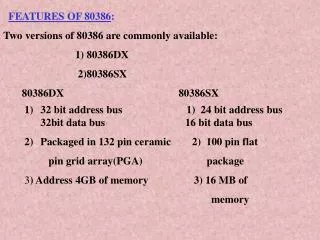
80386DX. Features of 80386DX. It supports 8/16/32 bit data operands It has 32-bit internal registers It supports 32-bit data bus and 32-bit non-multiplexed address bus It supports Physical Address of 4GB Virtual Address of 64TB Maximum Segment size of 4GB. Features of 80386DX.

E N D
Features of 80386DX • It supports 8/16/32 bit data operands • It has 32-bit internal registers • It supports 32-bit data bus and 32-bit non-multiplexed address bus • It supports • Physical Address of 4GB • Virtual Address of 64TB • Maximum Segment size of 4GB
Features of 80386DX • It operates in 3 different modes • Real • Protected • Virtual 8086 • MMU provides virtual memory, paging and 4 levels of protection • Clock Frequency : 20,25 and 33MHz • It has 132 pin package
Architecture of 80386 UQ: Draw the block diagram of the 80386 DX Processor and explain each block in brief
Architecture of 80386 • Three Sections: • Bus Interface units • Central Processing Unit • Memory Management Unit
Architecture of 80386 • The internal architecture of 80386 is divided into three sections: • Central Processing Unit • Memory Management Unit • Bus Interface unit
Central Processing Unit • The CPU is further divided into: • Instruction Unit • Execution Unit • Instruction Unit: • It decodes the opcode bytes received from the 16-byte instruction queue and arranges them into a 3-decoded instruction queue. • After decoding it is passed to control section for deriving necessary control signals
Central Processing Unit • Execution Unit: • It has 8 general purpose and 8 special purpose registers which either handles data or offset addresses. • The 64-bit barrel shifter increases the speed of all shift, rotate, multiply and divide operations • The multiply/divide logic implements the bit-shift-rotate algorithms to complete the operations in minimum time(Even 32bit multiplication is done in 1µs)
Central Processing Unit • Element of the EU • Arithmetic/logic unit (ALU) • Performs the operation identified by ADD, SUB, AND, etc. • Flags register • Holds status and control information • General-purpose registers • Holds address or data information • Control ROM • Contains microcode sequences that define operations performed by machine instructions • Special multiply, shift, and barrel shift hardware • Accelerate multiply, divide, and rotate operations
Memory Management Unit • MMU consists of a segmentation unit and paging unit • Segmentation Unit: • It allows the use of two address components - segment and offset – for relocability and sharing of code and data • It allows a maximum segment size of 4GB • It provides a 4-level protection mechanism for protecting and isolating system’s code and data from those of application program
Memory Management Unit • The limit and attribute PLA checks segment limits and attributes at segment level to avoid invalid accesses to code and data in memory segment. • Paging Unit • It organizes physical memory in terms of pages of 4KB size • It works under the control of segmentation unit • It converts linear addresses into physical addresses • The control and attribute PLA checks privileges at page level.
Bus Interface Unit • It has a prioritizer to resolve the priority of various bus requests. This controls the access of bus • Address driver drives the byte enable and address signals A2 – A31. • Pipeline/bus size unit handles the control signals for pipelining and dynamic bus sizing units • Data buffers interface the internal data bus with system bus
Signal Interface • Signals are arranged by functional groups. • The # symbol indicates active low signal. • When no # is present, the signal is active high. • Example: M/IO# - High voltage indicates memory selected • - Low voltage indicates I/O selected
Signal Interface • Clock (CLK2): • It is divided by two internally to generate the internal processor clock. • The clock can be synchronized to a known phase. • Data Bus (D0 through D31): • It has three-state bidirectional signals. • It can transfer data on 32- and 16-bit buses using a data bus sizing feature.
Signal Interface • Address Bus (A2 through A31) • Provides three-state outputs • It provides physical memory addresses or I/O port addresses. • It can access 4GB of physical memory from 00000000H to FFFFFFFFH • Only higher 30 are released by MP(Microprocessor) • A1 and A0 are used internally by MP to produce the four byte enable signals(BE3# -- BE0#)
Signal Interface • Byte Enable Outputs( BE0# -- BE3#) • enable 4 memory banks • indicates which bytes of the 32-bit data bus are involved with the current transfer. • BE0# applies to D0-D7 • BE1# applies to D8-D15 • BE2# applies to D16-D23 • BE3# applies to D24-D31 • No. of Byte Enables asserted indicates physical size of operand being transferred (1, 2, 3, or 4 bytes).
Signal Interface • Byte Enable Outputs( BE0# -- BE3#)
Signal Interface • Bus Cycle Definition Signals (W/R#, D/C#, M/IO# , LOCK#) • three-state outputs • W/R# :distinguishes b/w write and read cycles. • D/C# :distinguishes b/w data and control cycles. • M/IO# :distinguishes b/w memory and I/O cycles. • LOCK# :distinguishes b/w locked and unlocked bus cycles. It enables CPU to prevent other bus masters gaining control of system bus.
Signal Interface • Bus Cycle Definition Signals: These control signals are decoded by the bus control logic to decide which bus cycle to be performed
Signal Interface • Bus Control Signals(ADS#,READY#,NA#,BS16#): • indicates when a bus cycle has begun and allow other system hardware to control address pipelining, data bus width and bus cycle termination. • ADDRESS STATUS (ADS#) : indicates that a valid address is driven at 80386DX pins. • TRANSFER ACKNOWLEDGE (READY#) : indicates that the cuurent bus cycle is complete and bus is ready for next bus cycle. It is useful for interfacing slow peripherals
Signal Interface • NEXT ADDRESS REQUEST (NA#) : This is used to enable address pipelining. It indicates that the system is prepared to accept the next address even if the end of the current cycle is not being acknowledged on READY#. • BUS SIZE 16 (BS16#) : This input constrains current bus cycle to use only D0-D15 of data bus.
Bus Arbitration Signals (HOLD, HLDA) • BUS HOLD REQUEST (HOLD): • This input indicates some other device requires bus mastership. • HOLD must remain asserted as long as any other device is a local bus master. • HOLD is not recognized while RESET is asserted. (i.e. RESET has priority over HOLD) • HOLD is level-sensitive.
Bus Arbitration Signals (HOLD, HLDA) • BUS HOLD ACKNOWLEDGE (HLDA): • This output indicates 80386 has given control of its local bus in response to HOLD asserted and it is in Bus Hold Acknowledge state. • This state offers near-complete signal isolation • The other output signals (D0-D31, BE0#-BE3#, A2-A31, W/R#, D/C#,M/IO#, LOCK# and ADS#) are in a high-impedance state so the requesting bus master may control them.
Coprocessor Interfacing • Intel 387DX numeric coprocessor is I/O mapped. • As Intel386DX begins supporting a coprocessor instruction, it tests the BUSY# and ERROR# signals to determine if the coprocessor can accept its next instruction • Intel 387DX can be given its command opcode immediately
Coprocessor Interface Signals (PEREQ, BUSY#, ERROR#) • COPROCESSOR REQUEST (PEREQ) : • PEREQ stands for Processor Extension Request. • This input signal indicates a coprocessor request for a data operand to be transferred to/from memory by the Intel386 DX. • PEREQ is level-sensitive
Coprocessor Interface Signals (PEREQ, BUSY#, ERROR#) • COPROCESSOR BUSY (BUSY#) : • This input indicates that coprocessor is still executing an instruction and is not yet able to accept another. • BUSY# is level-sensitive
Coprocessor Interface Signals (PEREQ, BUSY#, ERROR#) • COPROCESSOR ERROR (ERROR#) : • This input signal indicates that the previous coprocessor instruction generated a coprocessor error of a type not masked by coprocessor's control register. • ERROR# is level-sensitive
A2-A31 (800000F8H) IO# D0-D31 (opcode) 80386 80387
A2-A31 (800000F8H) IO# D0-D31 (opcode) PEREQ A2-A31 (800000FCH) 80386 80387 IO# D0-D31 (operand)
A2-A31 (800000F8H) IO# D0-D31 (opcode) PEREQ A2-A31 (800000FCH) 80386 80387 IO# (Coprocessor is busy computing floating point operation) D0-D31 (operand) BUSY#
A2-A31 (800000F8H) IO# D0-D31 (opcode) PEREQ A2-A31 (800000FCH) 80386 80387 IO# (floating point operation error (which is not masked)) D0-D31 (operand) BUSY# ERROR#
Interrupt Signals (INTR, NMI, RESET) • MASKABLE INTERRUPT REQUEST (INTR): • This input indicates a request for interrupt service, which can be masked by Flag Register IF bit. • When processor responds to INTR input, it performs two interrupt acknowledge cycles and at the end of second, it latches an 8-bit interrupt vector on D0-D7 to identify source of interrupt. • INTR is level-sensitive • To assure recognition of an INTR request, INTR should remain asserted until the first interrupt acknowledge bus cycle begins.
Interrupt Signals (INTR, NMI, RESET) • NON-MASKABLE INTERRUPT REQUEST(NMI): • This input indicates a request for interrupt service which cannot be masked by software. • The NMI request is always processed according to the pointer or gate in slot 2 of the interrupt table. • Because of fixed NMI slot, no interrupt acknowledge cycles are performed. • NMI is rising edge-sensitive • Once NMI processing has begun, no additional NMIs are processed until the next IRET instruction.
Interrupt Signals (INTR, NMI, RESET) • RESET (RESET) : • This input signal suspends any operation in progress and places the Intel386 DX in a known reset state. • The Intel386 DX is reset by asserting RESET for 15 or more CLK2 periods • When RESET is asserted, all other input pins are ignored, and all other bus pins are driven to an idle bus state. • RESET is level-sensitive
Signal Interfaces Table 5-3. Idle Bus State During Reset
Signal Interfaces • Vcc: These are system power supply lines • GND: These are return lines for the power supply